Lec 02-20-2025: Sequential Circuits, Latches & Flip-Flops | CSCI 343
A combinational circuit has no memory, its output depends only on its current inputs. That’s fine for things like adders, but it means the circuit can’t remember anything between moments. Sequential circuits fix this by adding memory: the output depends not just on current inputs, but on past inputs too. This is what allows a circuit to have state — a stored value that persists and influences future behavior.
The memory in a sequential circuit is held in flip-flops, which store one bit each. A clock is a signal that oscillates between 0 and 1 at a regular rate — it acts as a heartbeat for the circuit, controlling when stored values are allowed to change and keeping everything synchronized.
Sequential Circuits
Section titled “Sequential Circuits”A synchronous sequential circuit is built around a feedback loop:
- External inputs feed into a combinational circuit
- The combinational circuit computes the outputs and the next state
- The next state gets stored in flip-flops on the next clock change
- The flip-flop outputs (the current state) feed back into the combinational circuit as additional inputs
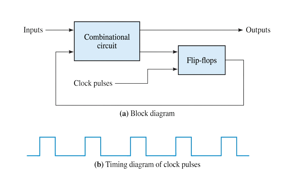
The clock timing diagram (part b) shows the regular square wave that drives this — state only updates at specific points in the clock cycle, so the circuit steps forward in discrete, predictable ticks rather than continuously reacting to every input change.
Finite State Machines
Section titled “Finite State Machines”A finite state machine (FSM), or automaton, is an abstract mathematical model of a sequential circuit. It has a finite number of inputs, outputs, and states — at each state of the computation, a transition function determines the next configuration based on a finite portion of the present configuration. At a high level, FSMs are the model that describes what a sequential circuit is doing, and flip-flops are the hardware that makes them possible.
There are two models for how outputs are produced:
Moore Machine
Section titled “Moore Machine”In a Moore machine, the output depends only on the present state.

Mealy Machine
Section titled “Mealy Machine”In a Mealy machine, the output depends on both the present state and the present input. This is different from Moore, where being in a given state always produces the same output no matter what — in a Mealy machine, the same state can produce different outputs depending on what input arrives. Edges are labeled as input/output pairs.

RS Latch/Flip-Flop
Section titled “RS Latch/Flip-Flop”The most basic memory element is the RS latch or flip-flop, built from two cross-coupled NOR gates. It has two inputs — Set () and Reset () — and two complementary outputs and .

and are intended to be complementary outputs — when one is , the other is .
The cross-coupling is what gives the latch memory: each gate’s output feeds back into the other gate’s input, so the circuit holds its last state even after the inputs return to 0.
The main behavior of the RS latch is as follows:
- Set (, ): forces ,
- Reset (, ): forces ,
- Hold (, ): and retain their previous values
- Forbidden (, ): both outputs are forced to (since a NOR gate with any input high outputs ), breaking the / complementary relationship. Worse, if and then return to at the same time, the final settled state is a race condition — which output wins depends on which gate’s feedback propagates first, so the result is indeterminate. This state must be avoided.
The characteristic table summarizes all possible input combinations and the resulting next state:
Clocked RS Latch/Flip-Flop
Section titled “Clocked RS Latch/Flip-Flop”A plain RS latch responds to inputs immediately, so any glitch on or can change the output. A clock input fixes this by acting as a gatekeeper — the resulting clocked RS latch/flip-flop only responds when clock = 1 (when the clock is high).

When clock = 0, both AND gates block the inputs and the clocked latch holds its state regardless of and . When clock = 1, the inputs pass through:
Once we understand what the clocked latch does, we can abstract away the internal gates and represent it as a single block — inputs on the left, outputs on the right:

This box notation is the standard way to represent flip-flops in circuit diagrams. The small triangle on the left edge marks the clock input, indicating the element only responds on the clock.
The clock gates the inputs but doesn’t remove the forbidden state — , with clock=1 is still undefined. That limitation is what motivates the D flip-flop next.
D Flip-Flop
Section titled “D Flip-Flop”The clocked RS latch still has the forbidden state problem. The D flip-flop eliminates it by having just one input D, where and are wired internally — since and are always opposites, the forbidden state can never occur.


The D flip-flop has the simplest characteristic table of any flip-flop — the output just follows the input:
JK Flip-Flop
Section titled “JK Flip-Flop”The JK flip-flop is an extension of the RS flip-flop that eliminates the forbidden state. acts like Set and acts like Reset, but when both and (which was forbidden in RS), the flip-flop simply toggles — flips to whatever it wasn’t. This makes the JK flip-flop the most versatile of the common types.

The , case is what sets JK apart — instead of a forbidden state, it toggles :
T Flip-Flop
Section titled “T Flip-Flop”The T (Toggle) flip-flop has a single input . When the output holds; when the output toggles. It’s essentially a JK flip-flop with and tied together, and is particularly useful for building counters.

The toggle behavior is the simplest possible: holds, complements: