Lec 03-20--04-01: Datapath Notes | CSCI 343
Execution Cycles
Section titled “Execution Cycles”Running an instruction is broken into a fixed sequence of stages, and every instruction goes through the same stages in the same order. Each stage does one part of the work and uses a different piece of hardware: fetching the instruction, decoding it and reading registers, computing in the ALU, accessing memory, and finally writing the result back to a register. The datapath we build in the rest of these notes is just the hardware that moves an instruction through these stages.
-
- Fetch
- Instruction memory (read only)
- Get in with an address
- The address is stored in the PC register
- Get out with the instruction
- PC register is updated to
- Decode
- The instruction is parsed into fields
- Get the source data
- Register file (2 read and 1 write port)
- Execute
- ALU: compute logical and arithmetic operations
- Output: result of the operation, it can represent the effective address (
lw,sw) - Also produces the check for zero flag (used by
beq)
- Memory access
- Data memory (read or write)
- Write back
- Register file
- The result (of reading memory or ALU computation) is written into the destination register
From Patterson
Section titled “From Patterson”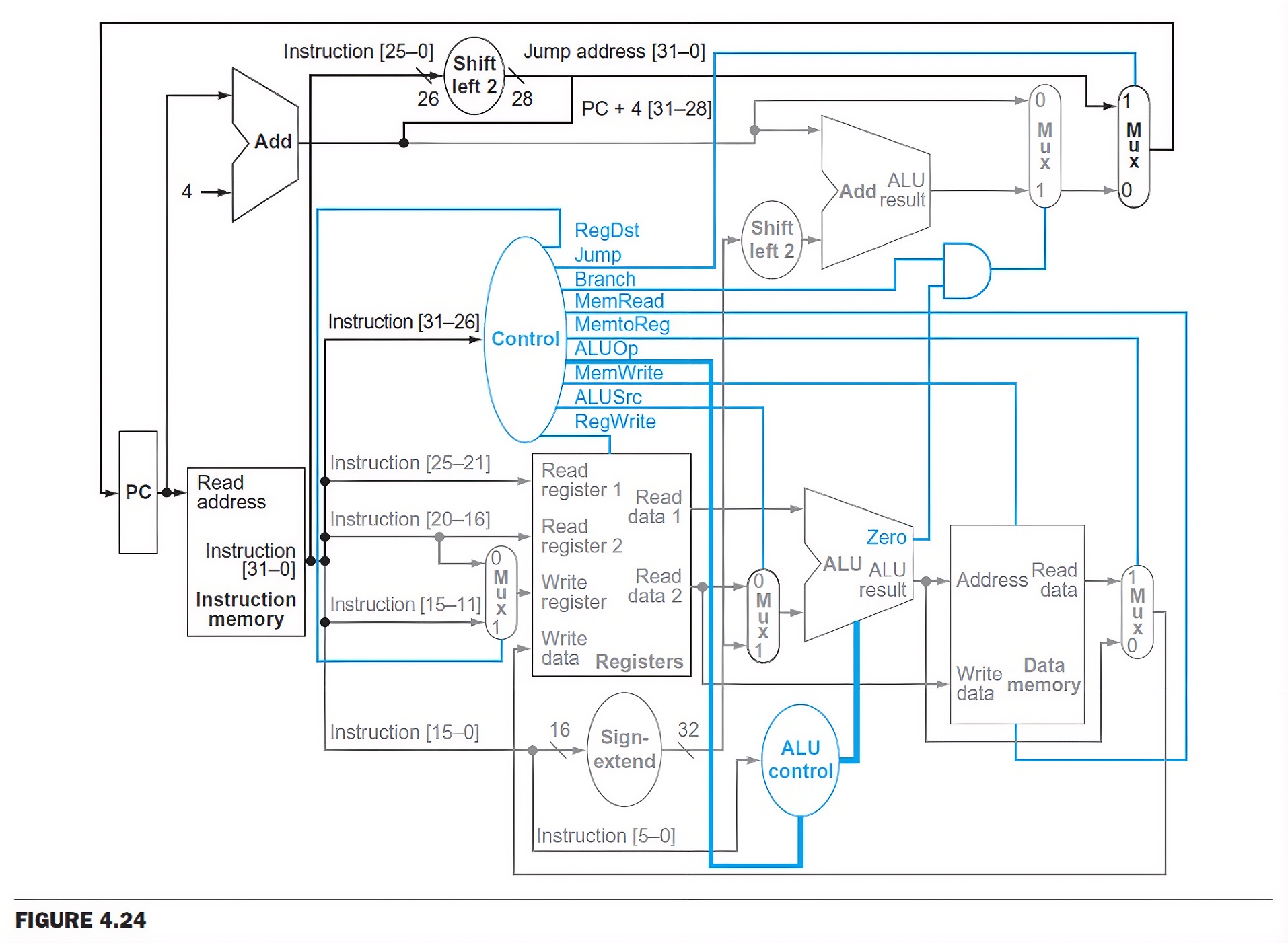
Datapath for R-format
Section titled “Datapath for R-format”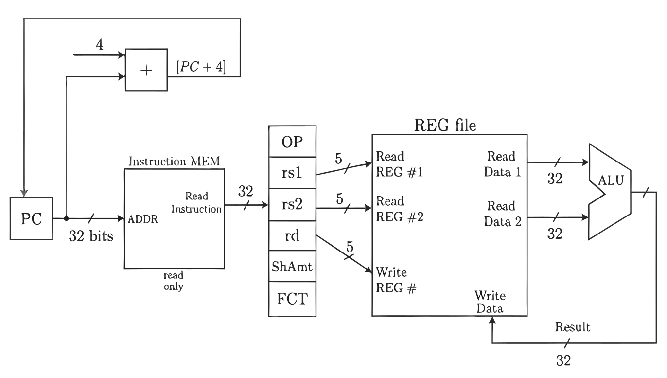
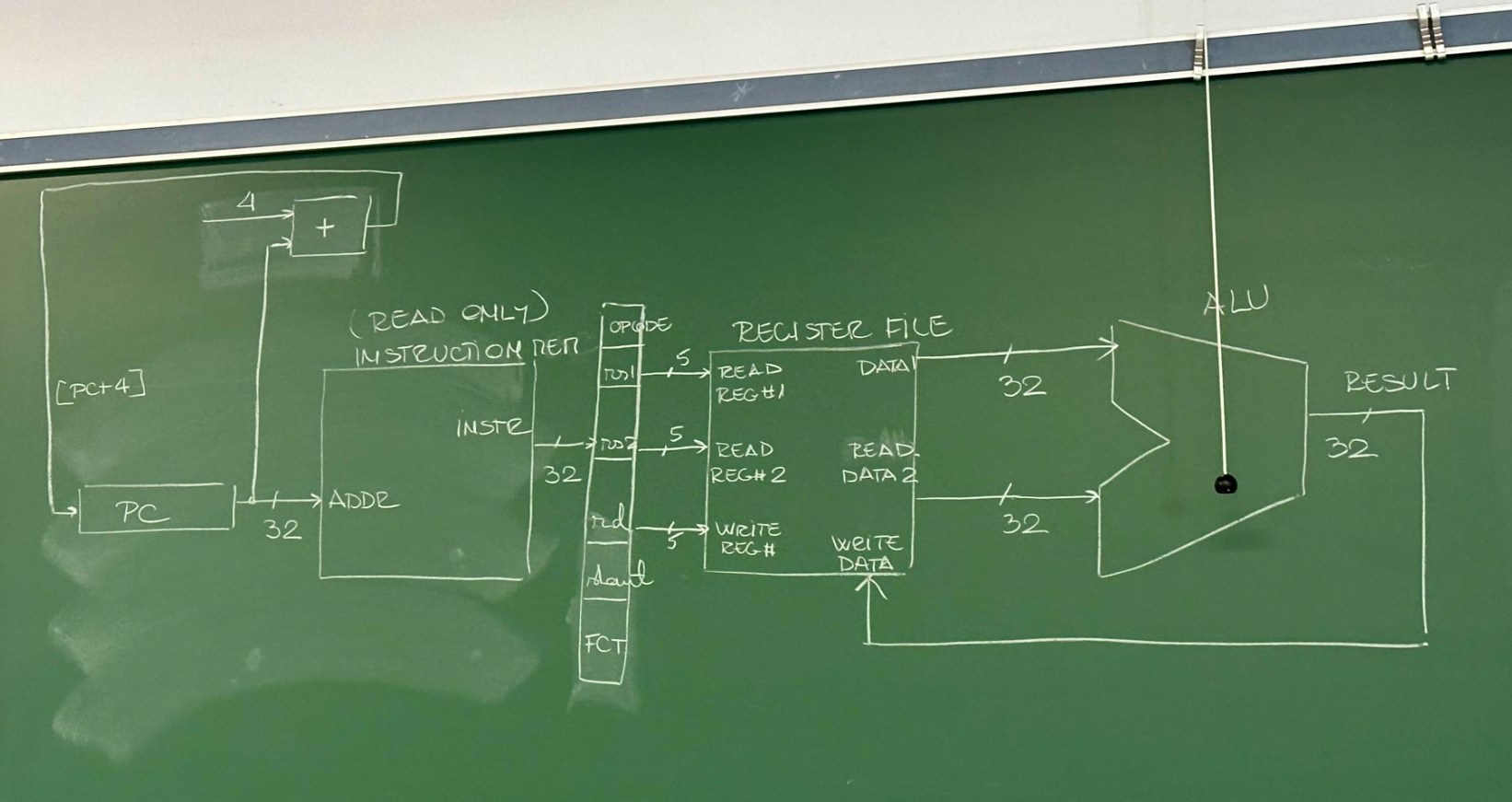
An R-format instruction (eg. add, sub) reads two registers, runs them through the ALU, and writes the result back into a third register:
-
- The instruction is fetched from instruction memory using the address in the PC, and the PC register is updated to .
- The instruction is decoded by splitting it into its fields (OP,
rs1,rs2,rd,ShAmt,FCT). - The two source registers are read: the
rs1field selects which register is read on port Read REG #1, andrs2selects the register read on Read REG #2, producing the two 32-bit operands on Read Data 1 and Read Data 2. - Both operands are passed into the ALU, which computes the operation and outputs a 32-bit result.
- The result is routed back to the Write Data port of the register file and written into the destination register
rdduring the write-back phase.
The fields wire into the register file as follows:
rs1(rs) → Read REG #1:- Read the value stored in register
rs1
- Read the value stored in register
rs2(rt) → Read REG #2:- Read the value stored in register
rs2
- Read the value stored in register
rd→ Write REG #:- Selects which register the result is written to during the Write-Back phase.
Datapath for lw (Load Word)
Section titled “Datapath for lw (Load Word)”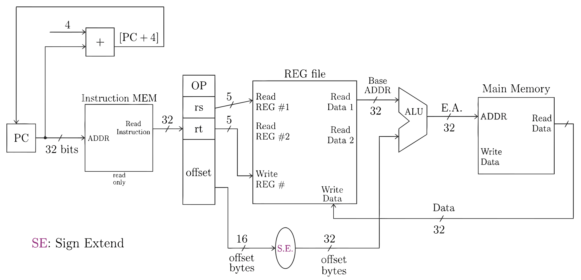
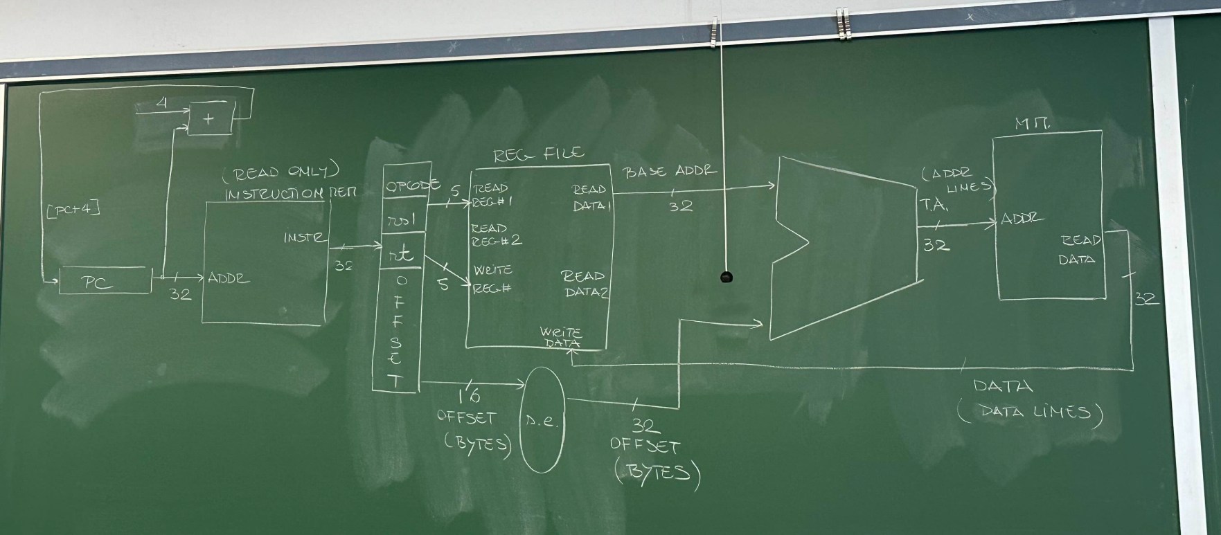
A lw instruction computes a memory address from a base register plus an offset, reads the word at that address out of main memory, and writes it into a destination register:
-
- The instruction is fetched from instruction memory using the address in the PC, and the PC is updated to .
- The instruction is decoded into its fields (OP,
rs,rt, offset). - The base register is read: the
rsfield selects which register is read on port Read REG #1, so the base address appears on Read Data 1. In parallel, the 16-bit offset is sign-extended to 32 bits by the S.E. unit because MIPS addresses are 32 bits wide. - The base address and the sign-extended offset are passed into the ALU and added together to produce the effective address (EA).
- The effective address is sent to the ADDR port of main memory, and the word at that location is read.
- The data read from memory is routed back to the Write Data port of the register file and written into the destination register
rtduring the write-back phase.
The fields wire into the register file as follows:
rs1(rs) → Read REG #1:- Read the base address stored in register
rs1
- Read the base address stored in register
rs2(rt) → Write REG #:- For
lw,rtis the destination, so it selects which register is written to during the Write-Back phase
- For
Datapath for beq
Section titled “Datapath for beq”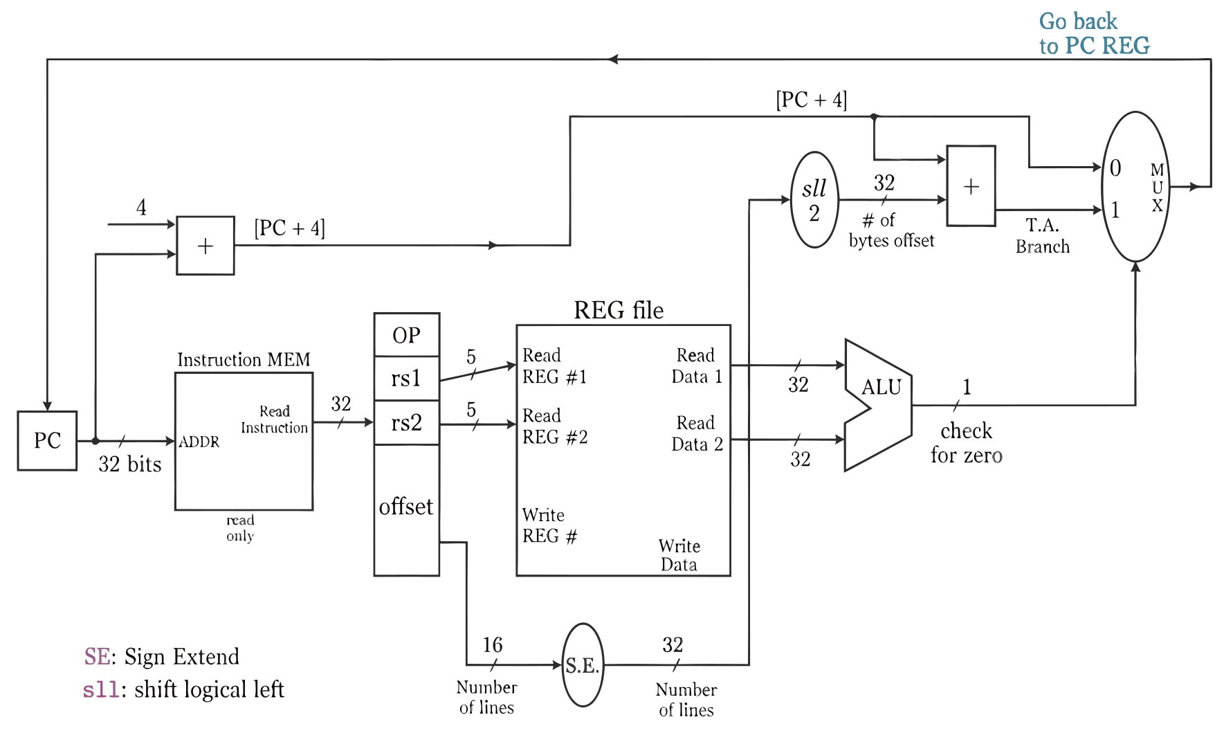
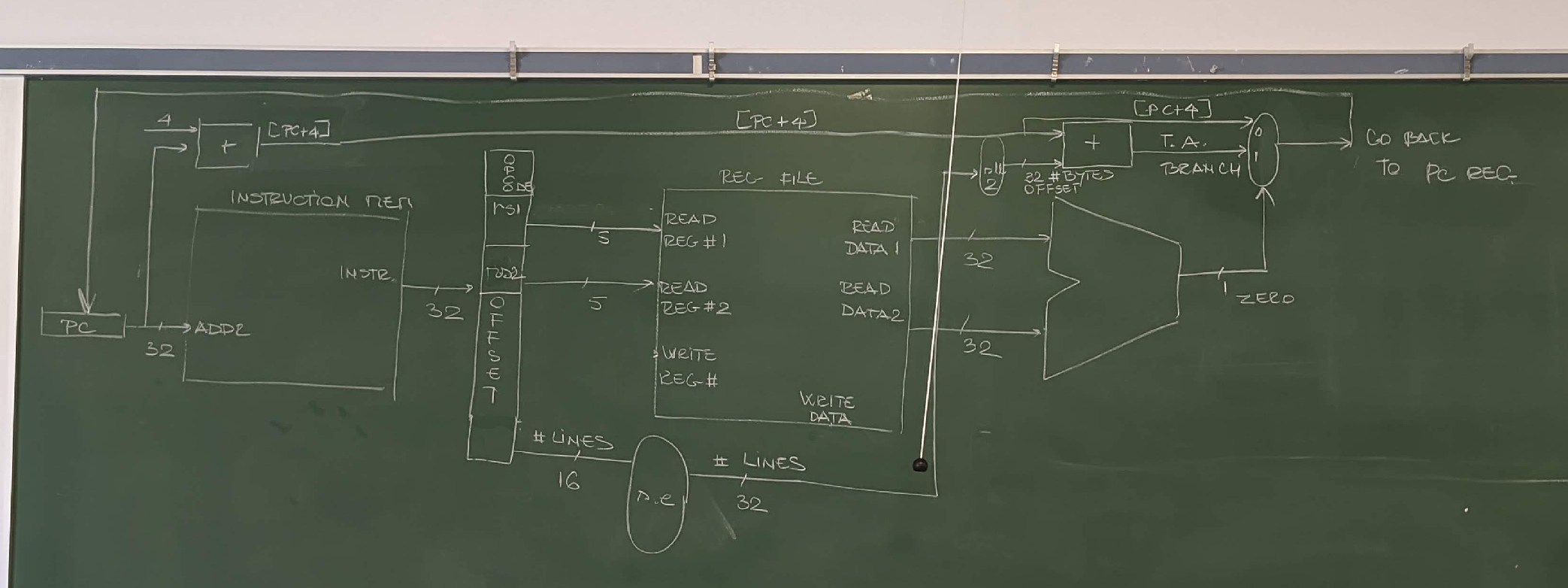
A beq instruction compares two registers and, if they are equal, redirects the PC to a branch target instead of falling through to :
-
- The instruction is fetched from instruction memory using the address in the PC, and the PC register is updated to .
- The instruction is decoded into its fields (OP,
rs1,rs2, offset). - The two registers being compared are read: the
rs1field selects which register is read on port Read REG #1, andrs2selects the register read on Read REG #2, producing the two operands on Read Data 1 and Read Data 2. - Both operands are passed into the ALU, which subtracts them and asserts the check-for-zero flag (1 bit) when they are equal.
- In parallel, the offset is sign-extended by the S.E. unit and then shifted left by 2 (
sll 2, see the note below). This byte offset is added to by the second adder to form the branch target address (T.A. Branch). - The MUX selects between and the branch target address. The check-for-zero flag controls the select line: if the registers were equal, the branch target is chosen and sent back to the PC register; otherwise the PC falls through to .
The fields wire into the register file as follows:
rs1(rs) → Read REG #1:- Read the value stored in register
rs1
- Read the value stored in register
rs2(rt) → Read REG #2:- Read the value stored in register
rs2
- Read the value stored in register
- No register is written, so the Write REG # / Write Data ports are unused
Register Field in Instructions
Section titled “Register Field in Instructions”- First register (Read Register 1): Bits
- Used by all instructions to read the first operand
- Second register (Read Register 2): Bits
- Used by:
- R-format instructions (eg.
add,sub) - store (
sw) to get the value to write memory - branch (
beq)
- R-format instructions (eg.
- Used by:
Write Registers
Section titled “Write Registers”- Load instruction (
lw)- Destination Register in bits
- R-format
- Destination Register in bits
Full Datapath With Control Lines
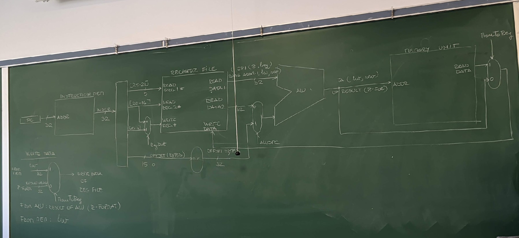
Section titled “Full Datapath With Control Lines”So far we have drawn a separate datapath for each instruction, but the hardware involved is one fixed circuit: there is only one ALU, one register file, one set of wires. Luckily the per-instruction datapaths above are nearly identical — they only disagree at a handful of spots where different instructions need a different value on the same wire. For example, the ALU’s second input is a register for R-format, but the offset for lw.
Wherever the instructions disagree, we add a multiplexer. Every value that some instruction might need is wired into the mux, and a control signal picks which one is actually used. So we don’t build a separate circuit per instruction; we build one circuit, and the control signals set the muxes so it acts in the manner that instruction needs.
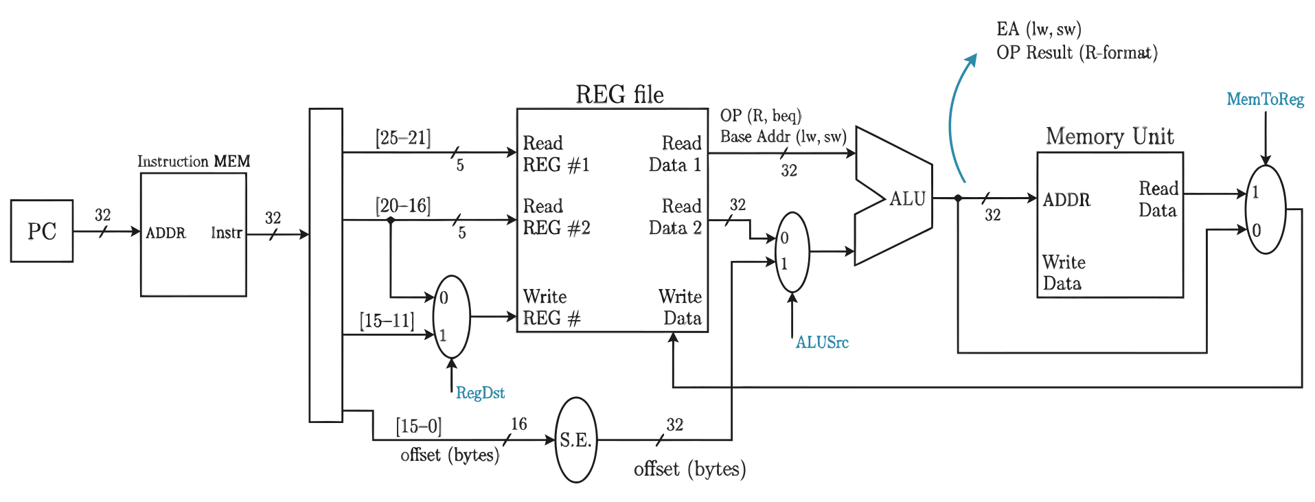
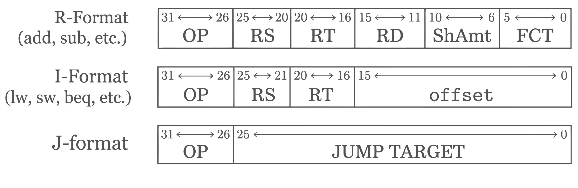
Each mux in the full datapath sits at one of those disagreement points, and each is paired with its own control signal. The three below cover the datapath choices: ALUSRC (what the ALU adds), RegDst (which register is written), and MemToReg (whether the written value comes from memory or the ALU). Looking at them one at a time makes it clear that picking an instruction’s behavior is nothing more than fixing the setting of each of these muxes. Several of these choices select an instruction field by its bit range, so the instruction formats are shown below for reference:
ALUSRC Mux
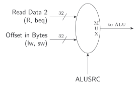
Section titled “ALUSRC Mux”Controls what the second input of the ALU will be, selecting between a register value and the sign-extended offset:
- For R-format and
beq, the second operand is Read Data 2, the value read from the register in bits . - For
lwandsw, the second operand is the 32-bit sign-extended offset (in bytes), used to compute the effective address.
The ALUSRC control line picks which input passes through: for lw/sw it selects the offset, and for R-format/beq it selects Read Data 2.
RegDst Mux
Section titled “RegDst Mux”Chooses which register field feeds the Write REG # port, i.e. which register gets written to.
- In R-format, the result is stored into
rd - In
lw, we load memory intortlw: Dest Reg in bits- R-format: Dest Reg in bits
The RegDst control line picks which input passes through: for lw it selects bits , and for R-format it selects bits .
![RegDst mux: input bits [20-16] (lw) and bits [15-11] (R-format), select line RegDst, output to Write REG #](/static/tex-svgs/f60b9c4080a9c6aa.svg)
MemToReg Mux
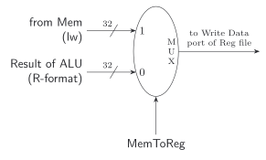
Section titled “MemToReg Mux”Chooses what value goes to the Write Data port of the register file:
- In
lw(input1), we write memory data into a register. - In R-format (input
0), we write the ALU computation result into the register.
The MemToReg control line picks which input passes through: for lw it selects the data read from memory, and for R-format it selects the ALU result.
Datapath for Jump
Section titled “Datapath for Jump”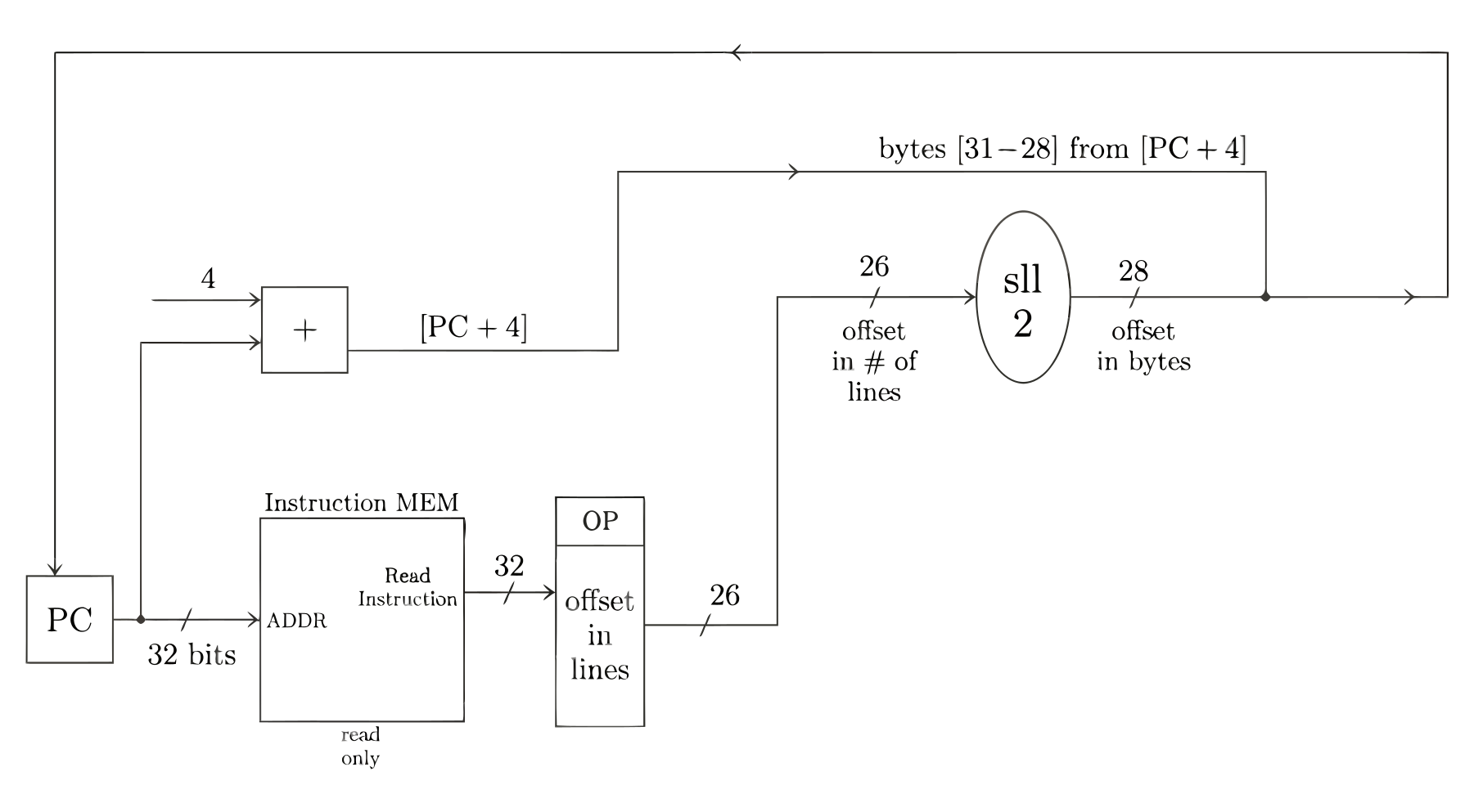
A jump instruction redirects the PC unconditionally to a target address, but the instruction only has room for a 26-bit address field while the PC needs a full 32-bit address. The target is reconstructed from that 26-bit field:
-
- The instruction is fetched from instruction memory using the address in the PC, and the PC register is updated to .
- The instruction is decoded into its fields (OP, 26-bit address).
- The 26-bit address field is shifted left by 2 (
sll 2) to recover the byte address, turning the 26 bits into 28. - The top 4 bits are still unspecified, so they are taken from . Concatenating these 4 bits with the 28 from above gives the full 32-bit jump target (
TA Jump). - The jump target is sent back to the PC register rather than .
No register or memory is accessed, so the register file and data memory ports are unused.
Control Logic for Updating PC Register
Section titled “Control Logic for Updating PC Register”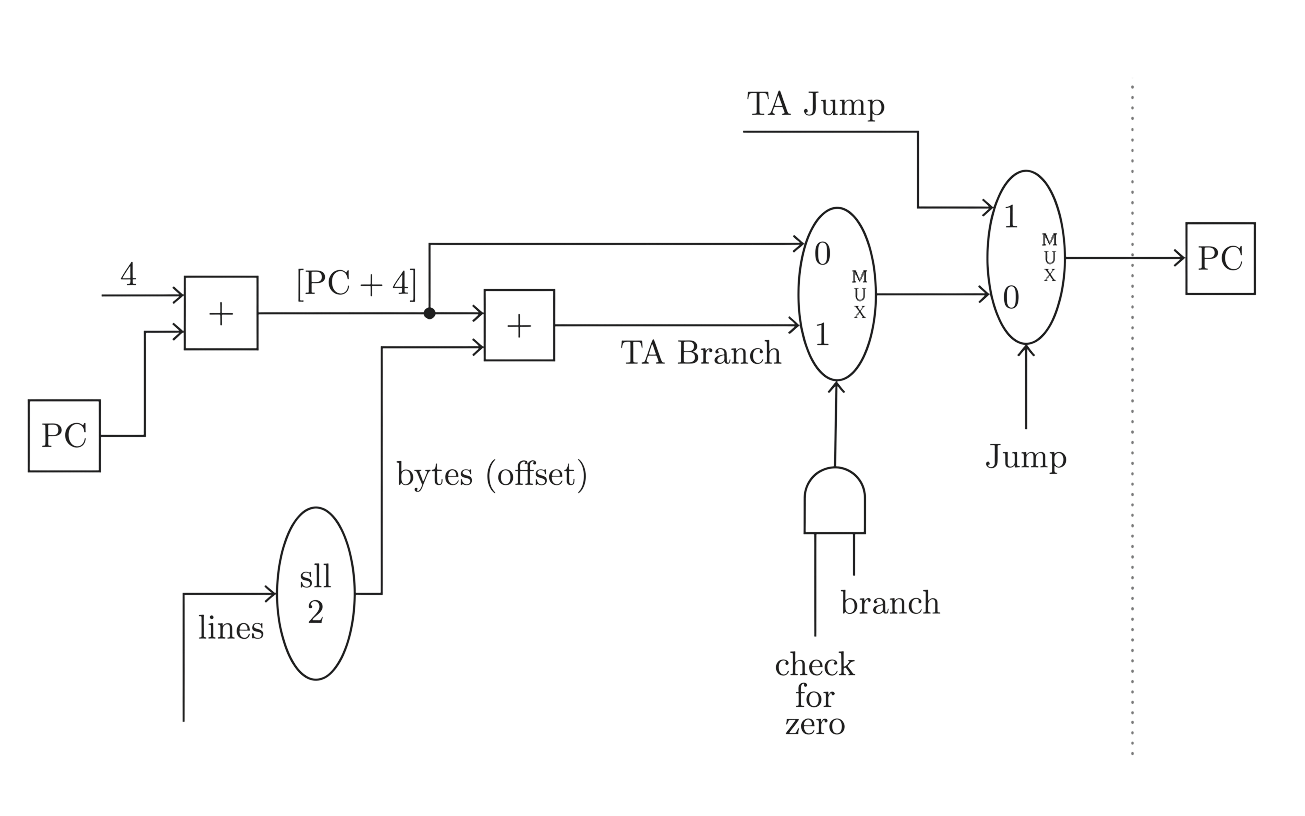
Most instructions just advance to ; only branches and jumps redirect the PC, and they redirect it for different reasons. A branch is conditional — it diverts only when the registers compared equal — while a jump is unconditional. Because these are two independent decisions, they are handled by two muxes in series rather than one: the first resolves “branch or not,” and the second resolves “jump or not,”. This is also why needs no control signal of its own, as it is simply what survives when neither mux is told to divert.
Each instruction type only has to set Branch and Jump to the right values, and the muxes route the correct next-PC value through to the PC register. We’ll look at each mux on its own below, then trace every instruction’s control values through both muxes in Tracing the Control Values Through Both Muxes.
PC Source / PCSrc
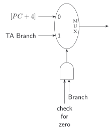
Section titled “PC Source / PCSrc”The first mux chooses between and the branch target address (T.A. Branch). Its select line comes from the AND of the Branch signal and the check-for-zero flag. Every instruction passes through this mux, but only a branch instruction can make it select T.A. Branch: for any non-branch instruction the Branch signal is 0, so the AND output is 0, allowing to pass through.
Jump Source
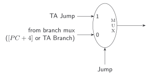
Section titled “Jump Source”This MUX sits downstream of PCSrc. This second mux chooses between T.A. Jump and the output of the branch mux (which is either or T.A. Branch). Its select line is the Jump signal.
Tracing the Control Values Through Both Muxes
Section titled “Tracing the Control Values Through Both Muxes”The input into the PC register depends on the control lines:
- Check for zero: 1 if
$s1 == $s2 - Branch: 1 if branch instruction
- Jump: 1 if jump instruction
The two muxes are chained: the branch mux (selected by check-for-zero AND Branch) feeds input 0 of the jump mux (selected by Jump). Below, each case traces the control values through both muxes to the value that lands in the PC register.
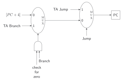
Using the single diagram above, we can trace each scenario through both muxes ( indicates that the signal’s value is irrelevant for that scenario):
R-format, lw, sw
check-for-zero=Branch= 0Jump= 0
PC gets .
beq with condition not satisfied
check-for-zero= 0Branch= 1Jump= 0
Since the AND gate outputs 0, PC gets (the branch is not taken).
beq with condition satisfied
check-for-zero= 1Branch= 1Jump= 0
Since the AND gate outputs 1, the branch mux selects T.A. Branch and PC gets the branch target (the branch is taken).
Jump
check-for-zero=Branch= 0Jump= 1
The branch mux passes , but the jump mux select line picks T.A. Jump instead, so PC gets the jump target.
Register File: Read & Write Port Implementation
Section titled “Register File: Read & Write Port Implementation”From Patterson Appendix:
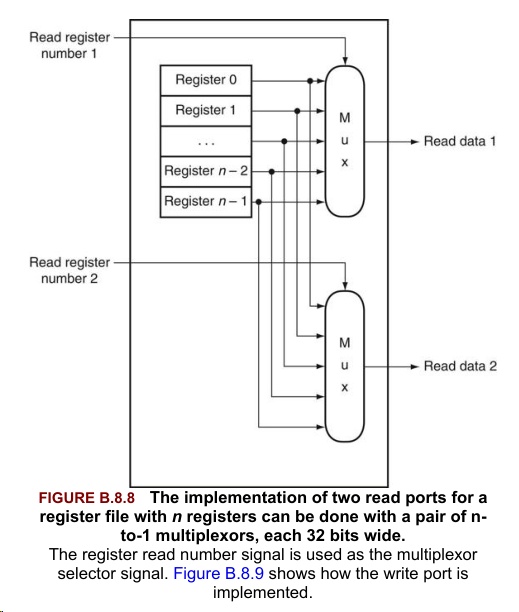
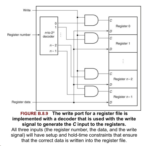
Read ports: each read port has its own dedicated multiplexer, with the data from all registers feeding into it as inputs. The input register number acts as the selector signal, and the output is the content of the selected register.
Write port: a decoder is used to enable only the target register based on the input register number. The write operation occurs on the clock edge, ensuring synchronization and preventing unintended changes to other registers.
This design allows the register file to support two simultaneous read operations and one write operation per clock cycle.
Datapath Control Signals
Section titled “Datapath Control Signals”The control signal receives the opcode (bits 31—26 of the instruction) and sets all relevant control lines to drive the datapath to perform the desired operation. These lines influence components such as multiplexers, the ALU, and memory units.
Control Signals by Instruction type
Section titled “Control Signals by Instruction type”Each instruction type (R-format, load, store, branch, jump) triggers specific settings in the control lines.
| R-format | Load | Store | Branch | Jump | |
|---|---|---|---|---|---|
| RegDst | 1 | 0 | |||
| MemToReg | 0 | 1 | |||
| ALUSRC | 0 | 1 | 1 | 0 | |
| Branch | 0 | 0 | 0 | 1 | 0 |
| Jump | 0 | 0 | 0 | 0 | 1 |
| RegWrite | 1 | 1 | 0 | 0 | 0 |
| MemWrite | 0 | 0 | 1 | 0 | 0 |
| MemRead | 0 | 1 | 0 | 0 | 0 |
The control signals group as:
- Mux: RegDst, MemToReg, ALUSRC, Jump, Branch
- Access: RegWrite
- Memory: MemWrite, MemRead
Note:
- indicates that the value is irrelevant for that instruction.
- RegDst determines the destination register (R-format uses
rd, load usesrt) - MemToReg selects source for register write (ALU result or memory)
- ALUSRC selects second ALU operand (register read vs. immediate)
Original Images:
Extra notes:
- For I-Format (eg. lw, sw, addi): the convention is to use EA as we’re calculating where in memory to read/write data.
- For I-Format branches (eg. beq, bne): the convention shifts to TA, since the immediate field (shifted left 2, sign-extended, added to PC+4) determines where execution continues, not a data address
- For J-format (j, jal): Always TA. The 26-bit field combined with the upper bits of PC+4 produces the jump destination — purely a control-flow target, never a data address