Design a Traffic Light using D Flip-Flops. Define 6 states (000 — 101):
state 0 (R/R) → state 1 (G/R) → state 2 (Y/R) → state 3 (R/R) → state 4 (R/G) → state 5 (R/Y)
Solution
We have 6 valid states encoded in 3 bits ABC: 000 through 101. States 110 and 111 are unused. The circuit has no external input — it simply cycles through the 6 states on each clock edge.
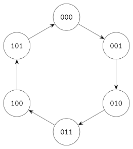
State Diagram:
Draw the state table:
The next state is fixed for each present state (no input variable), so the table has one row per state. The state sequence is given directly by the problem, so we fill in the Q(t+1) columns first (the unused states can optionally be included, filled in as Don’t Cares):
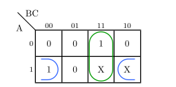
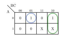
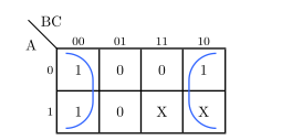
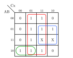
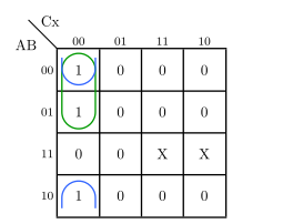
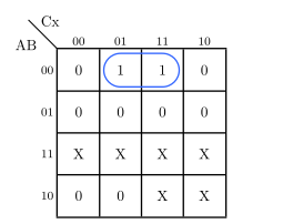
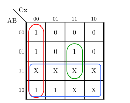
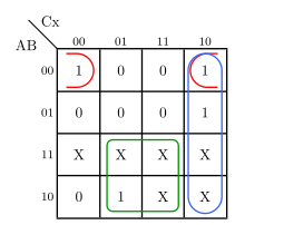
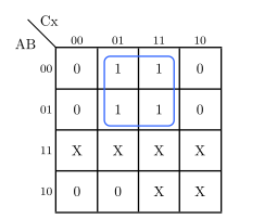
Unused states ABC = 110 and 111 are treated as Don’t Care conditions on the K-maps:
DA:
DA=BC+AC′
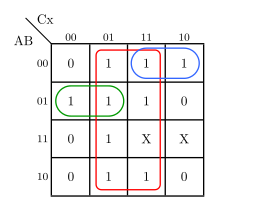
DB:
DB=BC′+A′B′C
DC:
DC=C′
Extending the Circuitry
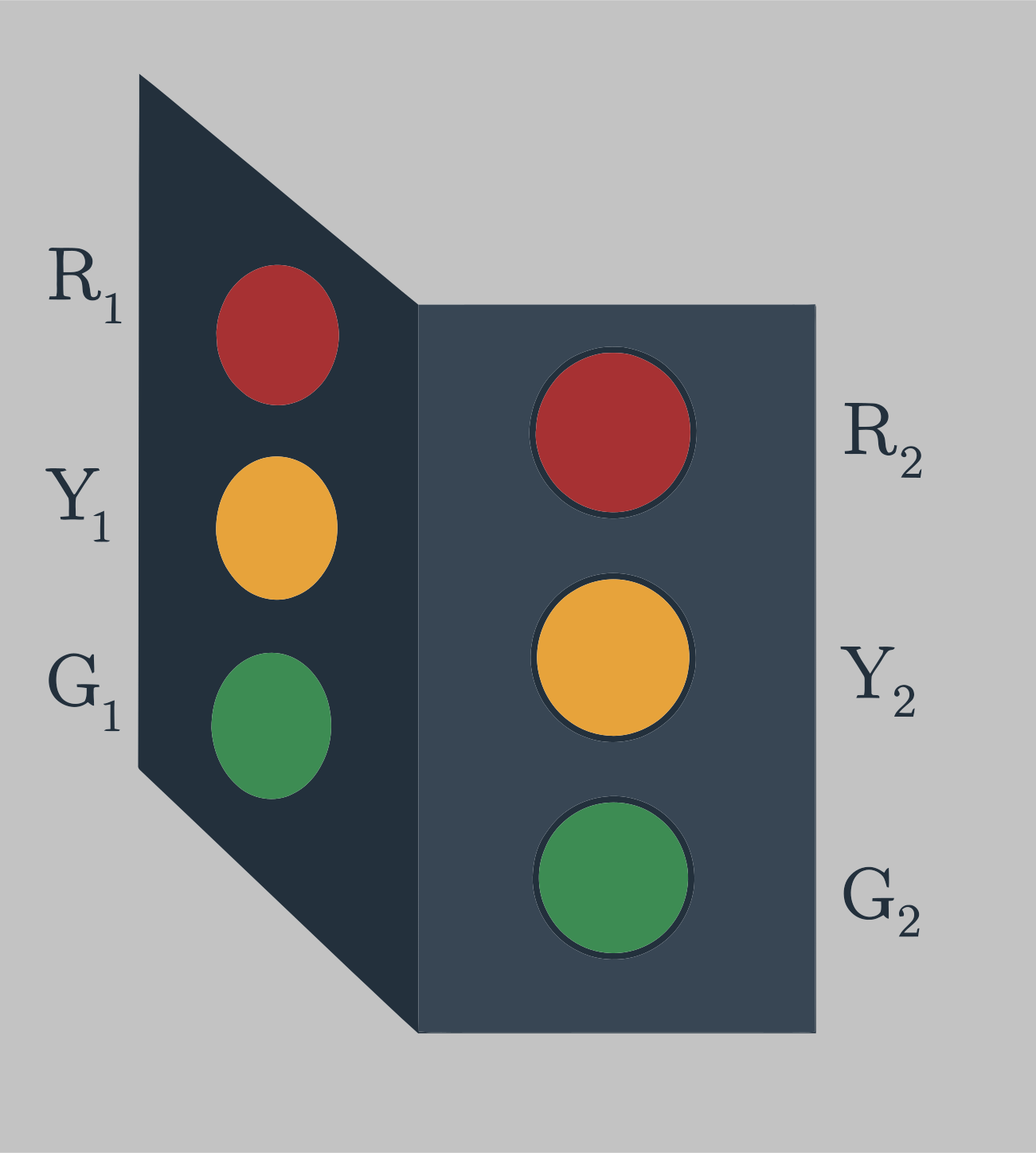
We can extend the circuitry by connecting the flip-flops to the traffic lights. Consider this cross-intersection traffic light, where both sides are controlled by the same flip-flops. To distinguish the lights on either side, we use subscripts: R1,Y1,G1 for Side 1 and R2,Y2,G2 for Side 2. Each state maps to a specific combination of active lights:
State
ABC
Side 1 / Side 2
0
000
R1/R2
1
001
G1/R2
2
010
Y1/R2
3
011
R1/R2
4
100
R1/G2
5
101
R1/Y2
6
110
unused
7
111
unused
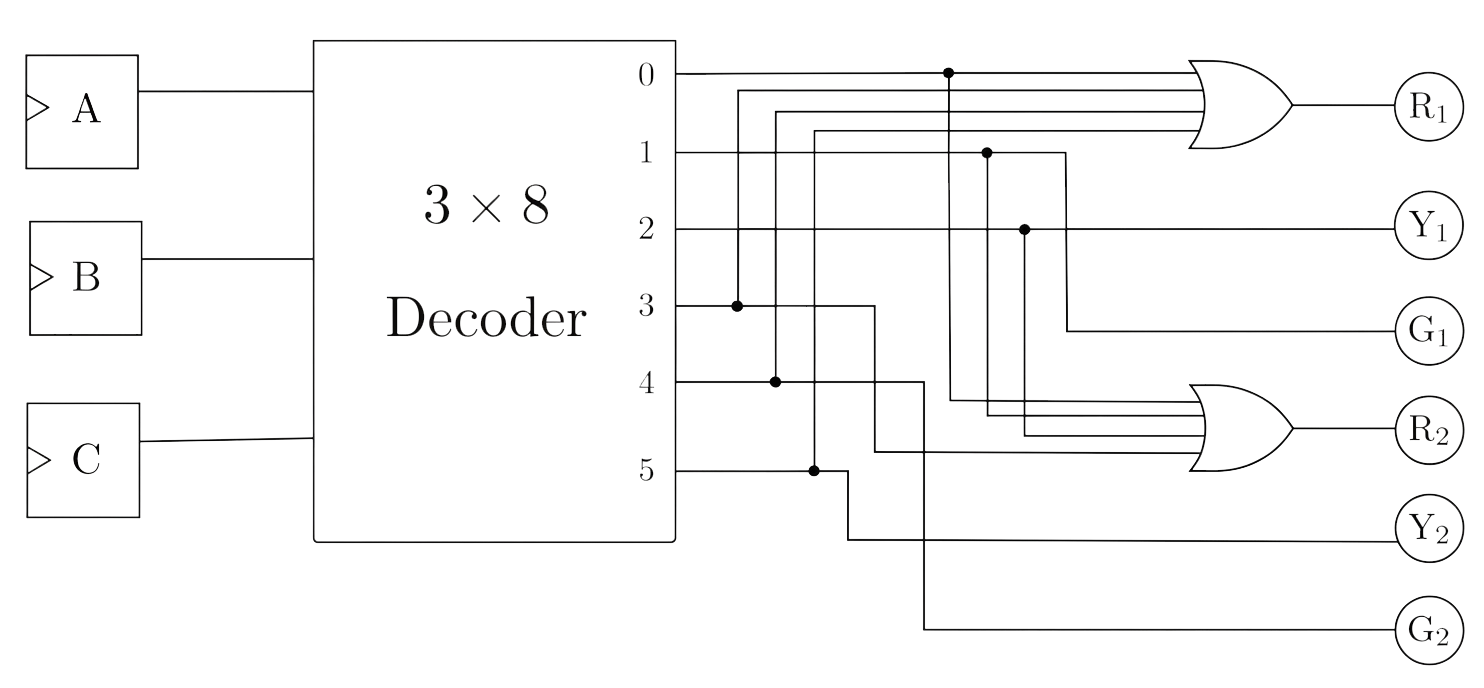
We can connect the flip flops to the lights with a 3×8 decoder, which takes a 3-bit input — each flip flop A, B, C contributing 1 bit — and enables exactly one of its 8 outputs.
We’ll use Dj to refer to decoder output j — that is, the wire that is enabled when the current state is j. We can’t wire a decoder output directly to a light, because some lights need to be on across multiple states (e.g. R1 is on in states 0, 3, 4, and 5). So those lights get an OR gate that combines the relevant decoder outputs for the states where that light should be on:
G1=D1
Y1=D2
R1=D0+D3+D4+D5 (red is on in states 0, 3, 4, 5)
G2=D4
Y2=D5
R2=D0+D1+D2+D3 (red is on in states 0, 1, 2, 3)
Decoder outputs D6 and D7 (for unused states 110 and 111) are left unconnected — they don’t feed into any light.
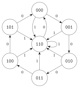
Consider the emergency state to be 110. We now have 7 states (0 to 6) and a 4-variable table for ABC and X. From the emergency state, x=1 stays in emergency and x=0 resets to 000. You can also consider that by 0/1 stays in the emergency state — in that case you will get different expressions for the f/f inputs.
Solution
We now have 7 valid states (000—110) and one input x, making this a 4-variable problem. State 111 is the only unused state.
The problem statement gives us a design choice — we’ll go with the one that returns to 000 from the emergency state when x=0.
Draw the state table:
Each state now has two rows — one for x=0 (normal cycling) and one for x=1 (go to emergency):
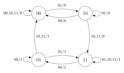
Each of the four present states AB becomes a node. Since there are two inputs x and y, each state has four outgoing edges labeled xy/Z:
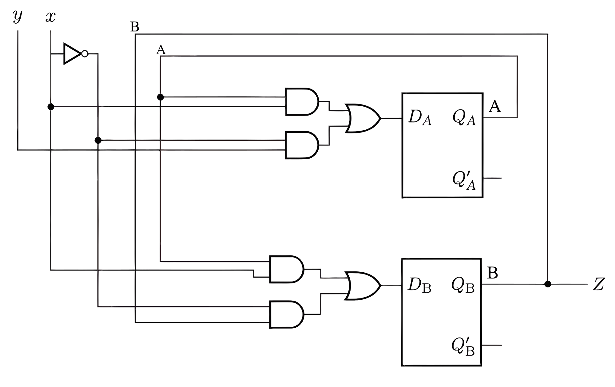
Draw the circuit:
In general, drawing the circuit requires knowing the f/f input expressions. You would derive them by filling in the DA and DB columns of the state table using the D flip-flop excitation table, then working through the K-maps to derive the minimized expressions.
In this problem, however, the next-state functions A(t+1) and B(t+1) are given directly. Because a D flip-flop passes its input straight through to its output — that is, D=Q(t+1) — the next-state function and the D input expression are one and the same. So the next-state expressions from the problem statement can be used directly as the D input expressions:
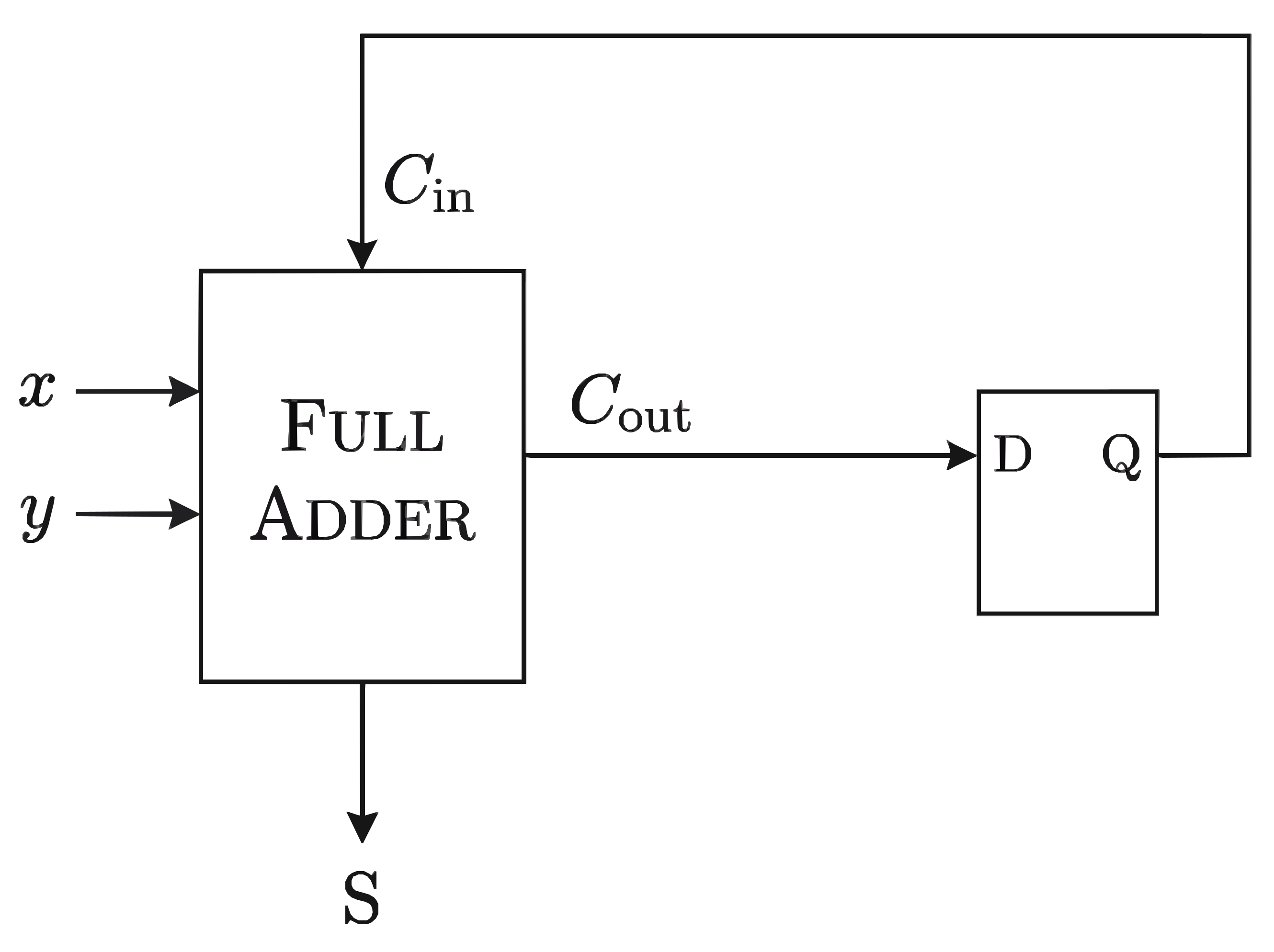
A sequential circuit has one f/f Q; two inputs, x and y; and one output S. It consists of a full adder circuit connected to a D f/f. Derive the state table and state diagram of the sequential circuit.
Hint
When adding two binary numbers, we add them one bit at a time (by column) and the carry that is generated by that addition will be remembered for the next one.
Solution
The circuitry that we build here is the adding core of a serial adder: it takes one bit from each number (x and y), produces their sum bit S, and passes the carry forward to the next pair.
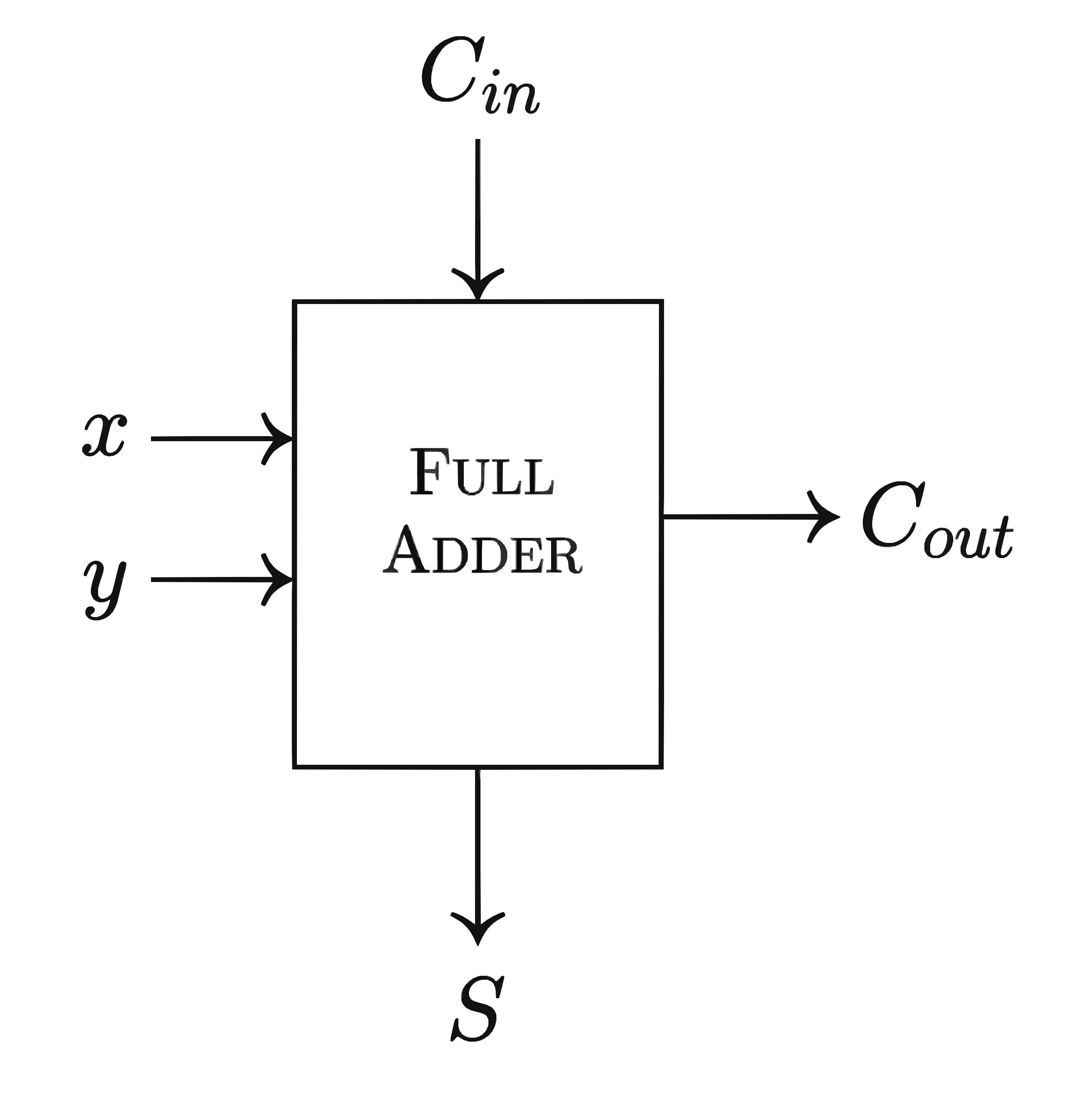
Recall the Full Adder:
A full adder takes 3 inputs: two addends (x and y) and the carry-in (Cin). Its outputs are the sum (S) and the carry-out (Cout).
Identify the role of the flip flop Q:
Each column’s addition produces a carry-out that has to be remembered, since it becomes the carry-in for the next column. So the circuit needs some way to hold onto a single bit of state between one addition and the next — and remembering a bit of state is exactly the job of a flip-flop. We feed the adder’s Cout into the flip-flop, and on the next addition it reappears at the flip-flop’s output, ready to serve as the Cin for that addition.
The carry-in to the adder is the current flip-flop state, Q.
The sum output of the adder is the circuit’s output S.
We know that the carry-out will be used as the next addition’s carry-in. We also know that by the characteristics of a D flip flop (D=Q(t+1)), its input will be exactly its output (the next state). So we can just compute the carry generated by the current addition and feed it into the flip flop’s input, and it will be available again as the next carry-in.
Draw the state table:
There is one flip-flop, so only two present states, Q=0 and Q=1. Each is paired with the four combinations of the inputs x and y:
For each row, we add the three bits Cin+x+y and split the 2-bit result across the two output columns:
The sum bit goes into the output S.
The carry bit is the Cout, which (as established above) is wired through the flip-flop to become the next state Q(t+1). So we just compute the carry bit from each row’s addition and fill it into Q(t+1).
As a sanity check, the rows match what the full adder should produce: the next state (the carry-out) is 1 exactly when at least two of {x,y,Q} are 1, and the output S is the XOR of the three bits.
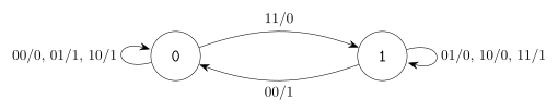
Draw the state diagram:
With a single flip-flop the diagram has just two nodes, Q=0 and Q=1, and each transition is labeled xy/S following the rows of the table above. For example, from Q=0 the inputs xy=11 generate a carry and move the circuit to Q=1 with output S=0.
Problem 5: Self-Correcting Sequential Circuit Design
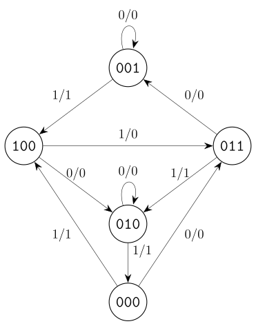
A sequential circuit has three f/f A, B, C; one input x; one output y.
Design the circuit using D f/f, treating unused states as don’t care conditions
Analyze if the circuit is self-correcting
Solution
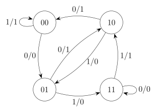
The transitions in the diagram are in the format input/output: the first value indicates the input variable driving the transition, and the second indicates the output of the circuit.
Draw the state table:
The state diagram tells us plenty of information upfront: the valid states, invalid states (the missing states), x input values that drive the transition for each state, and the output y for each transition. Using that information, we fill the state table (the unused states can optionally be included, filled in as Don’t Cares):
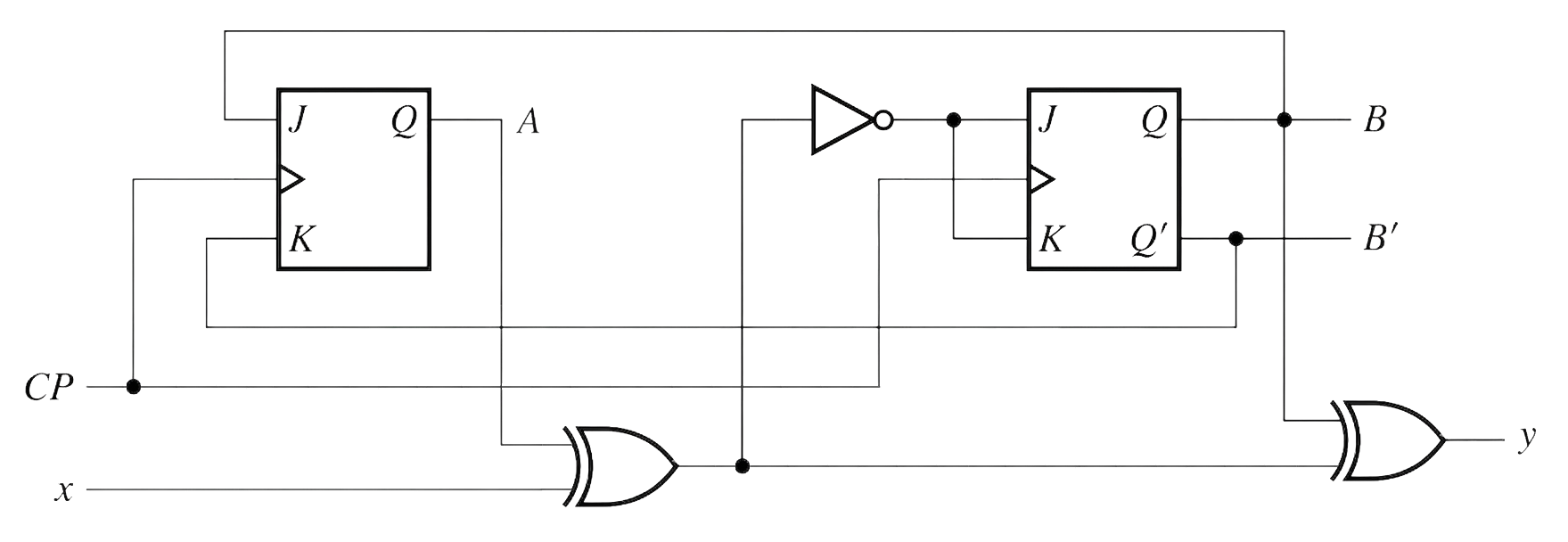
A sequential circuit has 2 JK f/f, one input x, and one output y. The logic diagram is shown below. Derive the state table and state diagram.
Solution
Get the expression of the f/f inputs (based on present states and external input) by tracing through the given circuit diagram. Based on present state and f/f inputs, get the next state.
With the f/f inputs in hand, each flip-flop’s next state follows from how a JK flip-flop behaves in response to its J/K inputs, as described by the JK characteristic table:
Draw the state diagram based on the state table. Each of the four present states AB becomes a node with a directed edge leading to the next state. The edges are labeled in the form x/y, where x is the input driving the transition and y is the resulting output:
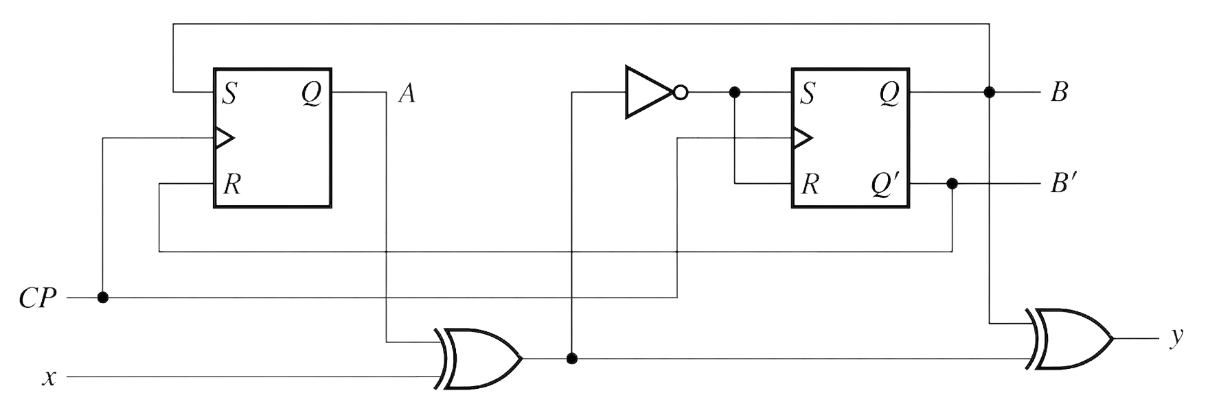
Problem 7: SR Flip-Flop Implementation of Problem 6’s Circuit
For flip-flop B: there are four rows where both S and R are 1, making B‘s next state undefined. This is a fundamental limitation of SR flip-flops compared to JK flip-flops — the JK design eliminates this invalid condition by toggling when both inputs are 1.
 Type of problems for Midterm 1 (Partial Solutions)