Lec 02-25-2025: Master-Slave Flip Flop, Registers & Clocked Sequential Circuit Design | CSCI 343
Master-Slave Flip Flop
Section titled “Master-Slave Flip Flop”In the previous lecture, we introduced clocked flip-flops, which are designed to only change state on a clock edge, but there’s still a problem when multiple flip-flops need to change state together. Consider a circuit with two flip-flops, A and B, that are supposed to swap states on the same clock edge:
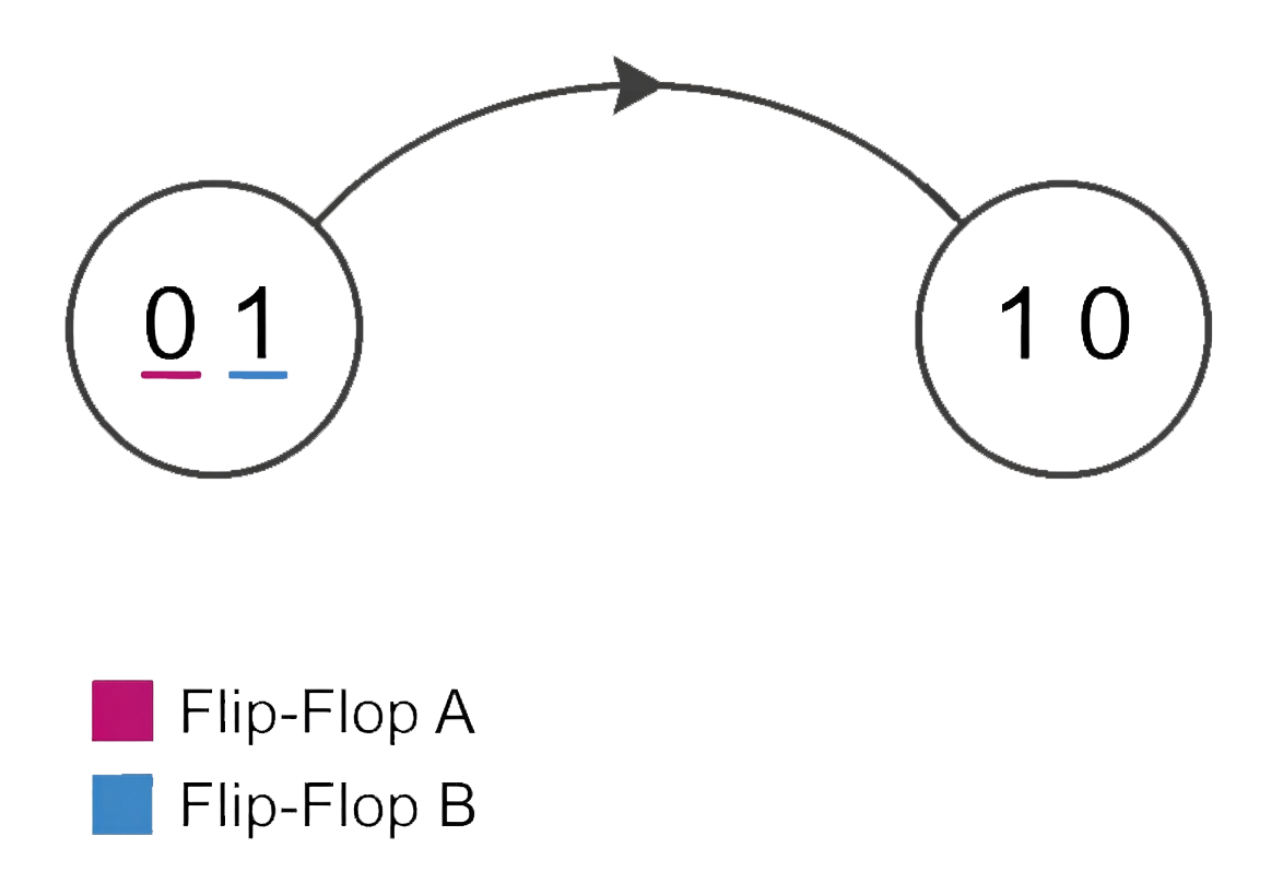
Each f/f must change state instantly at the same time, otherwise we might end up at the wrong state. For example, if A updates before B, then B might read A’s new value instead of A’s old value when computing its own next state, producing a wrong result.
The master-slave approach solves this by splitting each flip-flop into two stages. The first stage (master) captures the input during one clock phase, and the second stage (slave) transfers that captured value to the output during the opposite phase. This way, the output only changes after the input has already been locked in — the two stages can never interfere with each other.
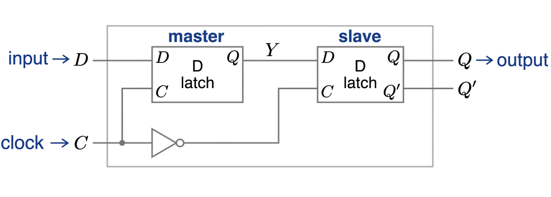
The master uses the clock directly, and the slave uses an inverted copy of the clock — so when the master is open (clock=1), the slave is locked, and vice versa. The output Q of the master (called Y) becomes the input to the slave.
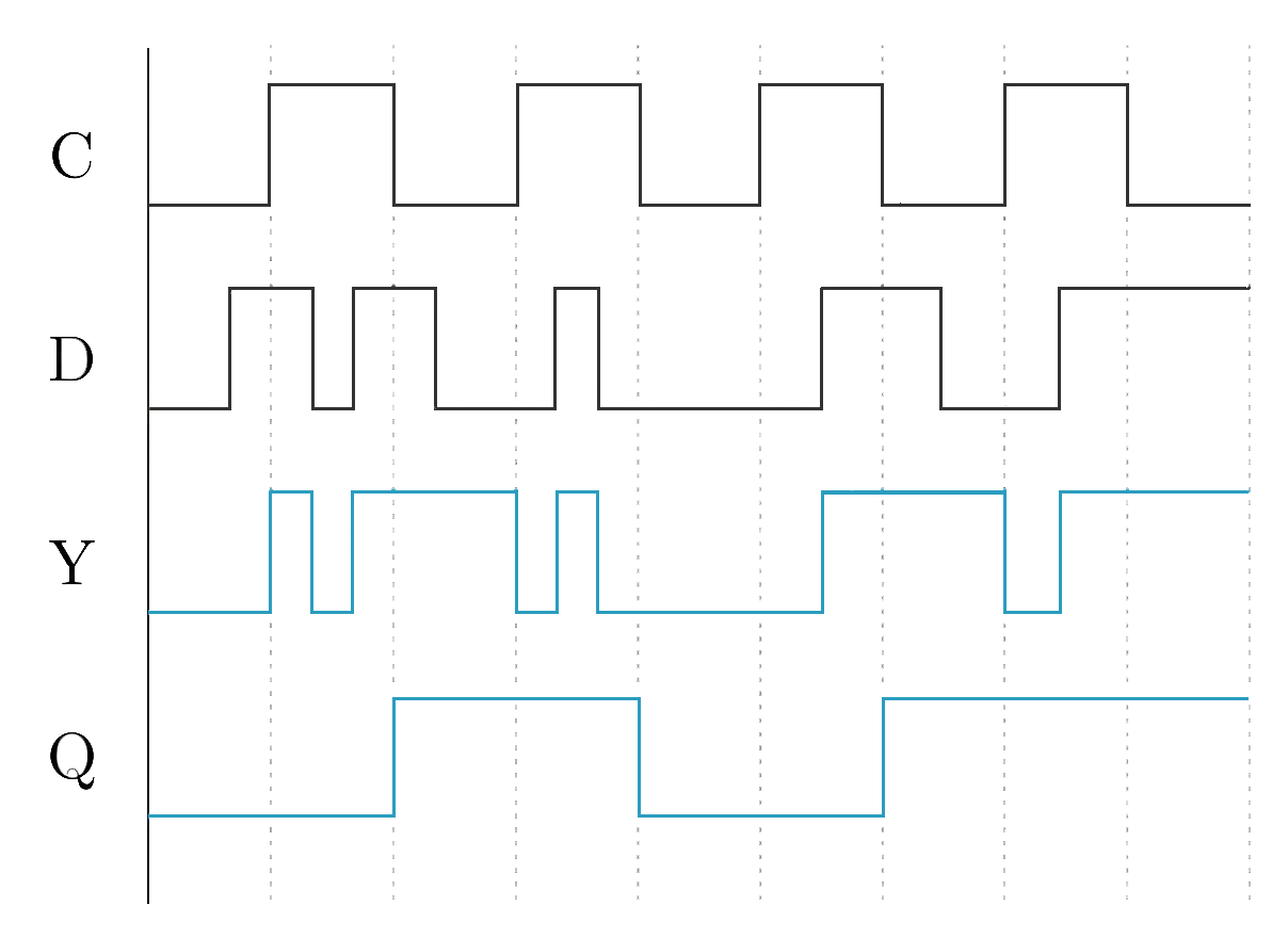
So the final output Q only ever changes on the falling edge of the clock (the transition from 1 to 0), which is when the slave unlocks and copies whatever Y was holding. The clock signal below shows this — the rising edge is where the master opens, and the falling edge is where the slave opens and Q updates:

When D and C are 1, Y follows D and the state of the master becomes 1. Once C drops to 0 (negative edge), the master locks in whatever Y was holding, and that is when the slave unlocks and copies Y into Q.
Given the signals for C and D, we can determine Y and Q by considering how they respond to the clock:
| Signal | clock = 1 | clock = 0 |
|---|---|---|
| Y | Copy of D | Holds last value |
| Q | Holds last value | Copy of Y |
Registers
Section titled “Registers”A register is a group of flip-flops that collectively store multiple bits of data. Since each flip-flop holds one bit, an -bit register is built from flip-flops sharing a common clock — all bits are captured simultaneously on the same clock edge, which is what the master-slave design was set up to ensure.
Parallel Register
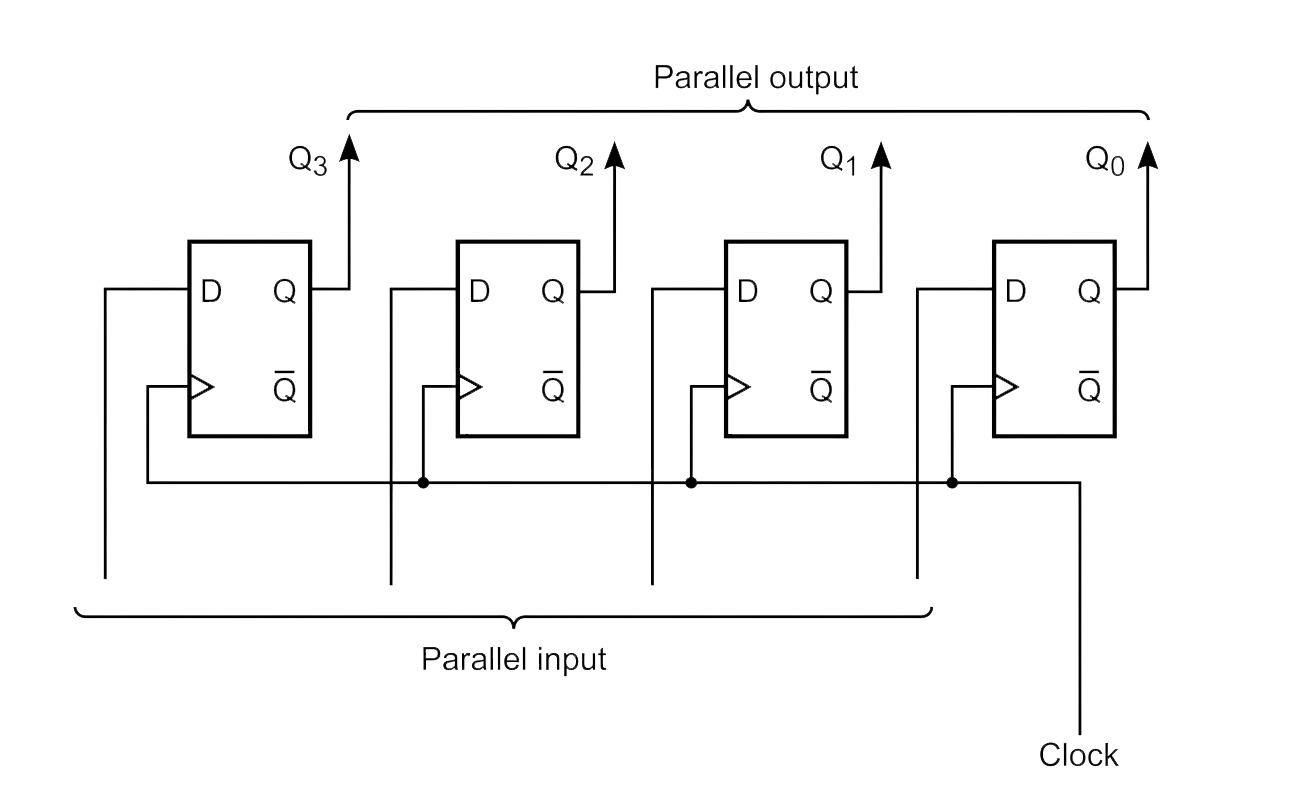
Section titled “Parallel Register”A standard 4-bit register using D flip-flops accepts all 4 bits of input at once (parallel input) and makes all 4 bits available simultaneously as output (parallel output):
Shift Register
Section titled “Shift Register”A shift register is capable of shifting its binary information to the right or to the left. All flip-flops receive a common clock pulse that causes the shift from one stage to the next:
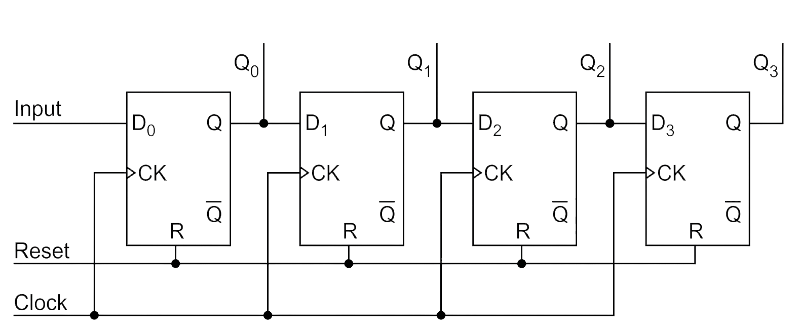
The input end is where new bits enter, and the output end is where bits fall off — the shift direction is simply determined by which end the input enters. Since the input enters at and the flip-flops are chained left to right (), each clock pulse pushes the entire chain one position to the right, and the bit at drops out.
Bidirectional Shift Register with Parallel Load
Section titled “Bidirectional Shift Register with Parallel Load”The most general shift register combines all modes into one circuit. Each stage uses a MUX to select between four possible operations, controlled by select lines and :
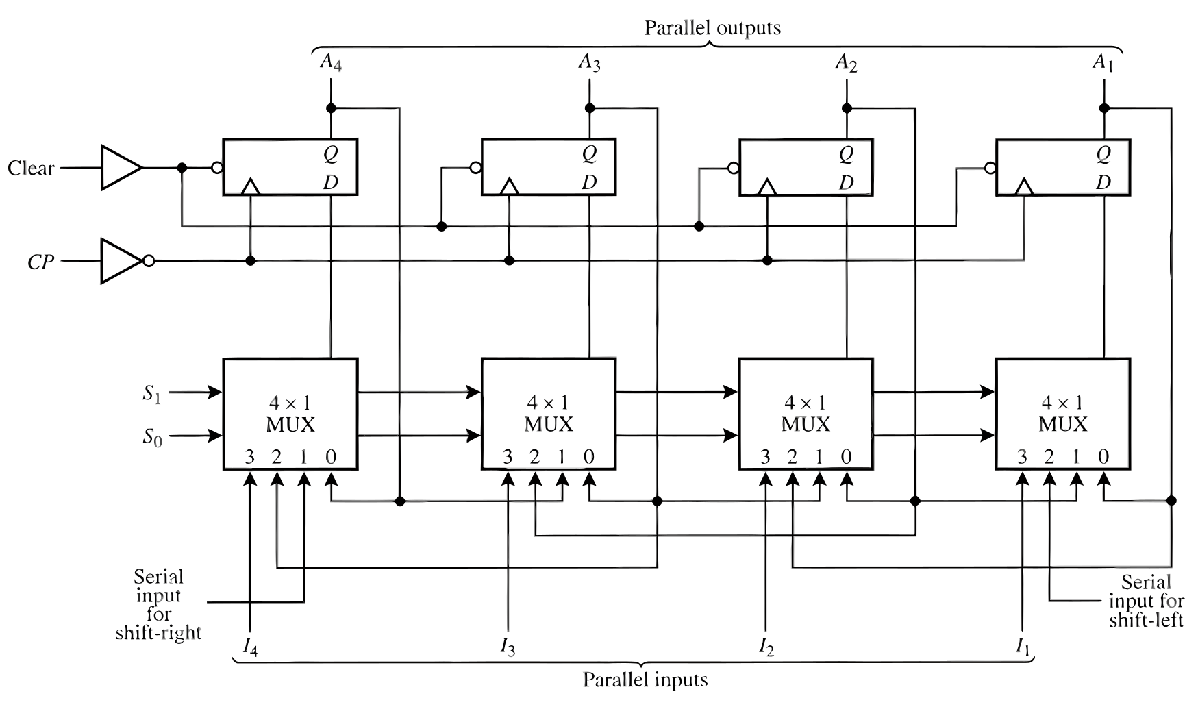
The most general shift register has the following functions:
-
- Clear control to clear registers to 0
- CP input for clock pulses to synchronize all operations
- A shift-right control to enable shift right operations
- A shift-left control to enable a shift-left operation
- A parallel-load control to enable a parallel transfer
- parallel output lines
- A control state that leaves the information unchanged even if the clock pulse is continuously applied
Designing a Clocked Sequential Circuit with JK Flip Flops
Section titled “Designing a Clocked Sequential Circuit with JK Flip Flops”Now that we know how flip-flops work, we can use them to design a circuit that implements a specific behavior from a state specification. The JK flip-flop is a common choice for this kind of design because of its flexibility in controlling state transitions, as is apparent from its characteristic table.
The process follows a standard recipe: write down the state transitions, figure out what J and K inputs are needed to produce each transition, then use K-maps to minimize the resulting Boolean expressions into circuit logic.
Say we want to design a clocked sequential circuit for the following specification using JK flip flops:
To draw the state diagram for these state rules, we’ll use the inputs as the transition functions (as edge labels). We can extrapolate the missing transitions as being “otherwise, stay in the same state” (i.e. self-loops on each state for where a transitiion wasn’t specified):
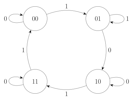
We use two flip-flops A and B to represent the four states (00, 01, 10, 11), with an input determining which transition to take.
The first step is to list every combination of present state and input (which we’ll call ), and look up the corresponding next state from the diagram:
The next step is to fill in the and columns. This is where the excitation table comes in. The characteristic table tells you what will be for a given and , but here we’re working in reverse: we already know and , and we need to figure out what and inputs would produce that transition. The excitation table gives us exactly that mapping:
The entries are don’t-cares. When the flip-flop is being set (), doesn’t matter, and vice versa. This is actually one of the reasons JK flip-flops are useful for this kind of design: the don’t-cares give the K-map minimization more flexibility later.
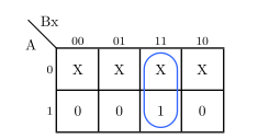
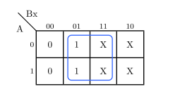
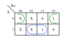
For each row in the state transition table, we apply the excitation table independently to flip-flop A and flip-flop B. Turning our focus on the first row for flip flop A, we’ll look at present state , next state , and , . Since current state of a is 0, and the next state of is at 0, then we look at the excitation table for where and , which tells us that in order to drive this transition, then must be 0 and can be anything (X). We repeat this process for every row and for both flip-flops, filling in the and columns:
K-Maps
Section titled “K-Maps”With the table filled in, we can minimize each of the four input expressions using K-maps. Each K-map has three variables: A, B, and .
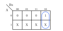
Circuit Diagram
Section titled “Circuit Diagram”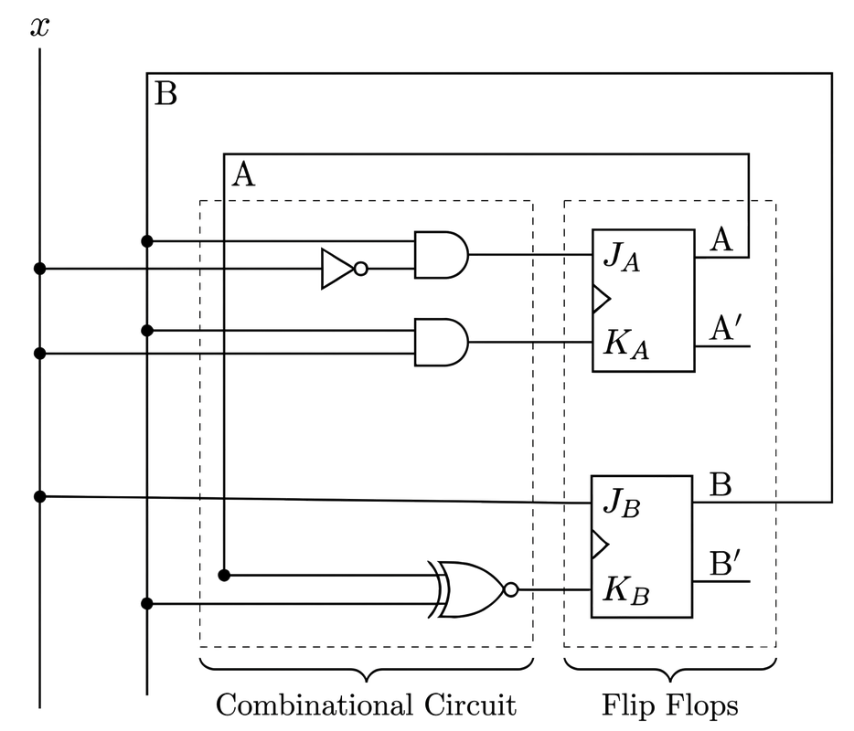
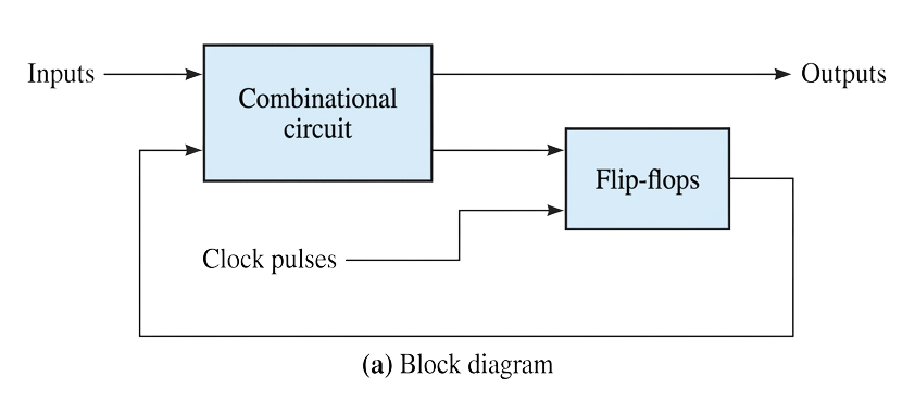
This is a concrete instance of the sequential circuit structure introduced in the previous lecture — the combinational logic gates on the left compute the next state from the current inputs, the two JK flip-flops on the right (acting as memory units) store the current state, and the feedback lines from back into the input bus are exactly the state feedback loop from the block diagram:
Characteristics & Excitation Tables
Section titled “Characteristics & Excitation Tables”The characteristic and excitation tables for each flip-flop type:
RS Flip-Flop (characteristic table):
RS Flip-Flop (excitation table):
D Flip-Flop (characteristic table):
D Flip-Flop (excitation table):
JK Flip-Flop (characteristic table):
JK Flip-Flop (excitation table):
T Flip-Flop (characteristic table):
T Flip-Flop (excitation table):