Lec 04-10-2025: Memory Hierarchy; Arrays of RAM | CSCI 343
Memory Structure
Section titled “Memory Structure”Memory is organized as a hierarchy of progressively larger units, each built from the one below it:
- A memory cell stores 1 bit — it’s the smallest unit
- 8 cells = 1 byte
- 4 bytes = 1 word (in MIPS)
- Words can be grouped into blocks
So building upward goes: cell byte word block. When you access memory, you work in the opposite direction: you start at the block level and drill down to the specific cell you need (block word byte cell).
The direction you drill down in depends on whether you’re reading or writing:
- Read — uses a MUX: given an address, a multiplexer selects and routes the data at that location to the output
- Write — uses a decoder: the address is decoded to activate exactly one specific location, so the incoming data gets written there and nowhere else
Memory Unit: Size and Structure
Section titled “Memory Unit: Size and Structure”A memory unit (one chip) is described by the notation , where:
- = address size — the number of bits in the address, which determines how many locations the chip has ( total)
- = word size — how many bits each location holds
For example, a (also written ) chip has 1024 addressable locations, each holding a 16-bit word.
A memory unit has a few standard lines going into and out of it:
- Read/write control line — tells the chip whether the current operation is a read or a write
- Input and output data lines — carry the data being written in or read out
- Select line — used in multi-chip setups to tell a specific chip “this operation is for you.” Without this, every chip would respond to every address, which would cause conflicts.
Addressing Modes
Section titled “Addressing Modes”The address a program uses can point to different granularities of data:
- Byte Addressing (used in MIPS): each address points to one byte. Since a word is 4 bytes, then consecutive words are at addresses 0, 4, 8, …
- Word Addressing: each address points to one word directly. Consecutive words are at addresses 0, 1, 2, …
Write/Read Operation
Section titled “Write/Read Operation”Write:
- Transfer the binary address of the desired word to the address lines.
- Transfer data bits that must be stored in memory to the data input lines.
- Activate the write control line.
Read:
- Transfer the binary address of the desired word to the address lines.
- Activate the read control line.
RAM: Types and Characteristics
Section titled “RAM: Types and Characteristics”Memory unit can be accessed to or from any desired random location — this is what makes it Random Access Memory (RAM). Any location can be selected at random and directly accessed.
There are two main technologies used to build RAM, each with their own trade-offs:
-
Static RAM (SRAM)
- Stores each bit using a flip-flop circuit, which actively holds its state as long as power is on
- Because the state is actively maintained, it doesn’t need refreshing
- Faster and more reliable, but flip-flops take more transistors, so SRAM is more expensive and less dense
- Used in cache memory, where speed matters most
-
Dynamic RAM (DRAM)
- Stores each bit as a charge on a capacitor — a 1 is a charged capacitor, a 0 is a discharged one
- Capacitors leak charge over time, which means the stored bits fade on their own. To prevent data loss, DRAM needs periodic refreshing: each location is read and immediately re-written to restore the charge
- This refresh overhead is the reason DRAM is slower, but capacitors are far simpler and smaller than flip-flops, so DRAM is much cheaper and denser — making it practical for main memory, where capacity matters more
Physical Characteristics
Section titled “Physical Characteristics”Both dynamic and static RAM are volatile — they lose their contents when power is removed. ROM (read only memory), which was covered in CSCI 240 or earlier, is a nonvolatile memory.
Array of RAM Chips
Section titled “Array of RAM Chips”Integrated-circuit RAM chips are available in a variety of sizes. If the memory unit needed for an application is larger than the capacity of one chip, it is necessary to combine a number of chips in an array to form the required memory size. The capacity of the memory depends on two parameters: the number of words and the number of bits per word. An increase in the number of words requires that we increase the address length. Every bit added to the length of the address doubles the number of words in memory. The increase in the number of bits per word requires that we increase the length of the data input and output lines, but the address length remains the same.
For example, consider a RAM chip:
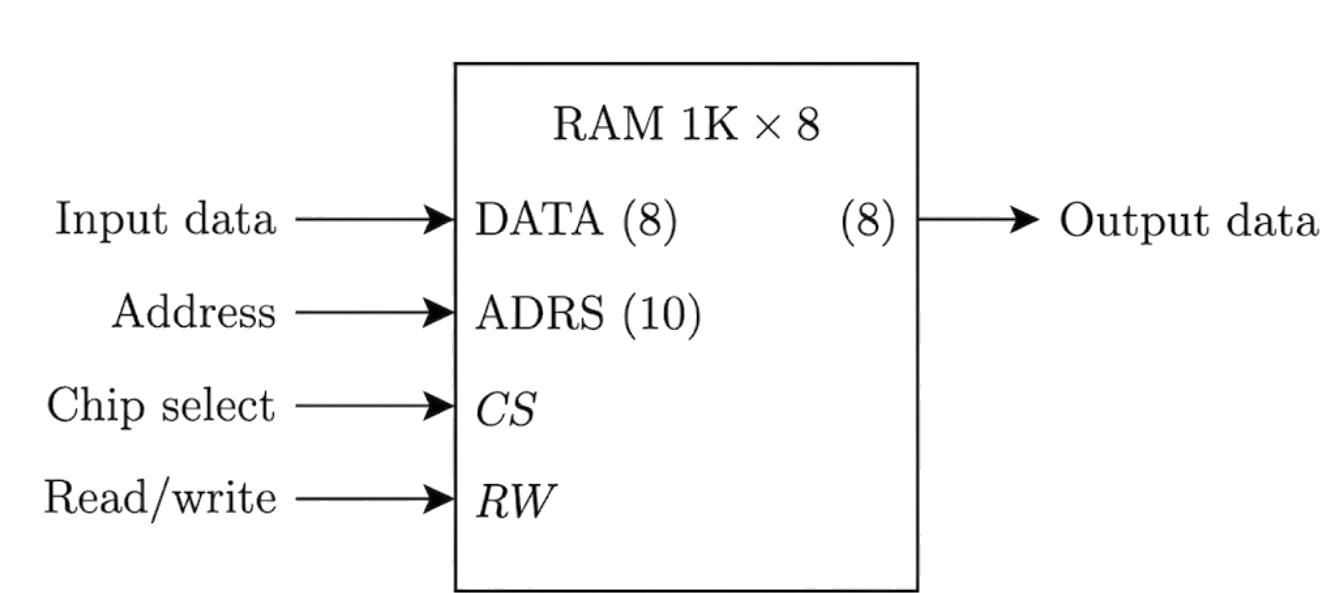
This chip has a capacity of 1024 words of 8 bits each: a 10-bit address, 8 input lines, and 8 output lines. CS (chip select) selects the particular RAM chip.
- Increasing the number of words in memory: every bit added to the address doubles the binary number that can be formed, which doubles the number of words.
- Increasing the size of the word: you can combine two chips to form a memory containing the same number of words but with twice as many bits in each word. For instance, if you want to be able to read and write words of size 16 bits instead of 8 bits, you’d combine two chips side by side.
Memory Hierarchy
Section titled “Memory Hierarchy”Structure that uses multiple levels of memories; as the distance from the CPU increases, the size of the memories and access time both increase.
| Level | Size / Capacity | Speed | Cost | Volatility |
|---|---|---|---|---|
| CPU — registers | small size, small capacity | very fast | very expensive | volatile |
| Cache (different levels) | small size, small capacity | very fast | very expensive | volatile |
| RAM | medium size and capacity | fast | affordable | volatile |
| Flash/USB memory | small size, large capacity | slower | cheaper | non-volatile |
| Hard drive | large size, very large capacity | slow | very cheap | non-volatile |
| Tape backup | large size, very large capacity | very slow | cheap | non-volatile |
There is a trade-off among key characteristics: cost, capacity, and access time.
Example: Expanding RAM with an Array of RAM Chips
Section titled “Example: Expanding RAM with an Array of RAM Chips”Given a RAM configuration , we want to:
- Increase the RAM capacity 10 times
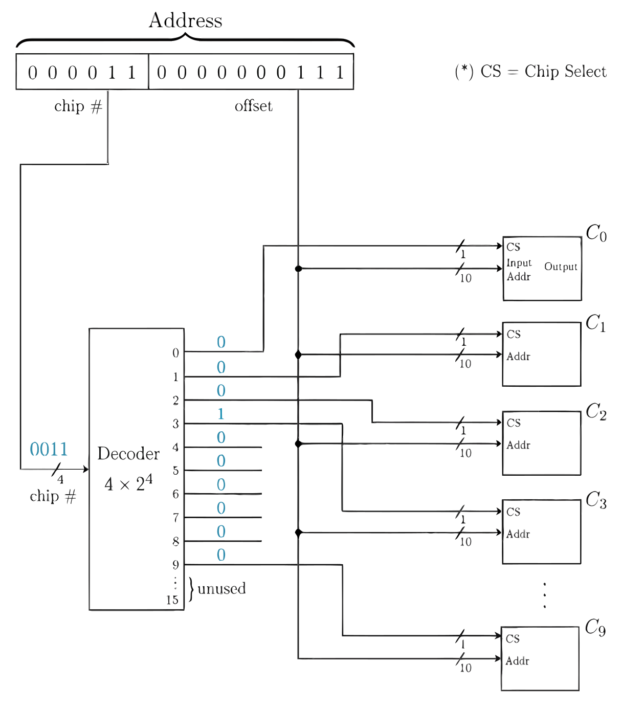
- Access word 3079 (draw the circuit and indicate the settings to accommodate this task)
To increase the capacity 10 times, we’ll put 10 chips together: through . Each chip still holds 1024 words, so the array holds 10240 words total.
Finding Which Chip Holds Word 3079
Section titled “Finding Which Chip Holds Word 3079”Since each chip holds 1024 words, words 0—1023 live on , words 1024—2047 on , and so on. To find which chip word 3079 belongs to, we divide:
So we need to access chip 3, at internal offset 7.
Building the Address
Section titled “Building the Address”We now need to figure out how to encode this as a binary address. Start by converting 3079 to binary:
Now, we go back and examine our chip config , which means each chip needs a 10-bit address to index any of its 1024 words. Since the words are 16 bits wide, we can assume a 16-bit address bus. That leaves bits unused by the offset — and those 6 upper bits are what we use to identify which chip to access.
So the address naturally splits into two fields:
Plugging in chip 3 (= ) and offset 7 (= ):
This matches the binary value of 3079 we computed above, which confirms the layout is correct.
Drawing the Circuit
Section titled “Drawing the Circuit”The upper 6 bits of the address tell us which chip to activate, so we use a decoder: it takes the chip number as input and enables exactly one output line, which connects to the CS (Chip Select) line of the corresponding chip.
We have 10 chips (0—9), so the decoder needs enough output lines to cover all of them. The smallest power of 2 that fits 10 outputs is , so we use a decoder. Since 10 fits perfectly well within 4 bits, only 4 of the 6 chip-select bits are ever needed to distinguish them — the remaining 2 upper bits of the field stay 0 and aren’t wired into the decoder. Outputs 10—15 of the decoder go unused.
Since our target word resides in , the input to the decoder will be (= ), which enables only output line 3, which leads to . All other output lines remain 0.