Lec 05-08-2025: Cache Performance | CSCI 343
Cache Performance
Section titled “Cache Performance”Cache is local memory, often with one or more levels “on chip” — access to data at “clock speed.” Effective cache management is important to improve performance of computer systems.
The cache is organized in the same way as the main memory: a given number of bytes in a word, and a given number of words in a block (possibly a given number of bytes / word). When data is accessed, the system checks if the data is already in the cache; if it is not in the cache, the entire block containing the requested address is copied to the cache. In MIPS data is referred to by its byte address, which is then broken down into the memory block in which it is stored, and its location within the block or word.
A machine cycle consists of the steps that a computer’s processor executes whenever it receives a machine language instruction. Modern CPUs are able to perform millions of machine cycles per second.
Clock rate: number of cycles your CPU executes per second, measured in GHz (gigahertz) — billions of cycles per second. The clock rate is useful for comparing the speed of chips made by the same company, but is not a reliable way to compare different types of computers because many other factors can determine the speed of a computer.
Clock Cycles and CPU Implementations
Section titled “Clock Cycles and CPU Implementations”Since cache performance is measured in clock cycles (hit time, miss penalty, and AMAT are all expressed this way), it helps to first review how instructions map to cycles under different CPU implementations.
Single Cycle CPU
Section titled “Single Cycle CPU”An implementation in which every instruction operates in 1 clock cycle of a fixed length.
Variable-Length Single Cycle CPU
Section titled “Variable-Length Single Cycle CPU”An implementation where every instruction executes in 1 clock cycle using a variable length clock, which for each instruction is only as long as it needs to be.
Multi Cycle CPU
Section titled “Multi Cycle CPU”Multicycle CPU where each stage of an instruction requires 1 clock cycle. Let us assume a classic RISC pipeline, with the following five stages:
- Instruction fetch cycle (IF).
- Instruction decode/Register fetch cycle (ID).
- Execution/Effective address cycle (EX).
- Memory access (MEM).
- Write-back cycle (WB).
Without pipeline: 5 clock-cycles / instruction
With pipelining: A new instruction is fetched every clock cycle by exploiting instruction-level parallelism — one could theoretically have five instructions in the five pipeline stages at once (one instruction per stage), so a different instruction completes stage 5 every clock cycle. On average, CPI = 1.
However, with a multiple-execution-unit processor, one may achieve even better CPI values ().
Cache Hits and Misses
Section titled “Cache Hits and Misses”CPU searches the cache and if there is a hit, it retrieves data from the cache. Sometimes data is not there (miss) and the data will need to be brought from lower memory, main memory (miss penalty).
Miss Penalty refers to the extra time required to bring the data into cache from the main memory whenever there is a “miss” in the cache.
The miss rate () is the fraction of memory accesses not found in the upper memory level.
Average Memory Access Time (AMAT)
Section titled “Average Memory Access Time (AMAT)”Example (Slide 38 — chapter 5)
Section titled “Example (Slide 38 — chapter 5)”Given:
- Hit time: 1 cycle (takes 1 cycle to get the data from cache 1)
- Miss penalty: 20 cycles (it takes 20 cycles to get data from main memory)
- I-cache miss rate: 5% (5 instructions out of 100 are not found in the cache)
- 1 clock cycle = 1ns hit time = 1ns
Multi-Level Cache
Section titled “Multi-Level Cache”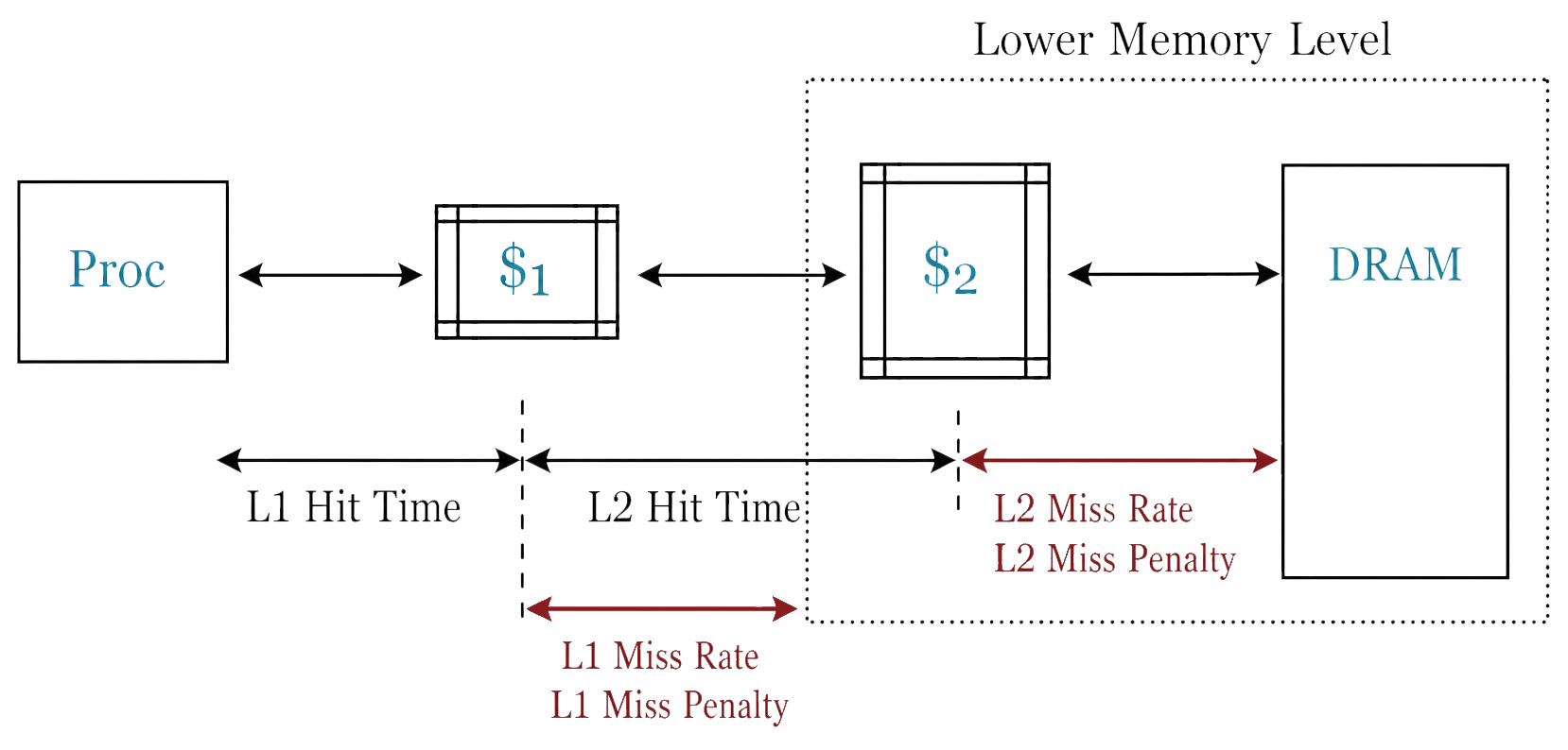
The first-level (L1) cache is small enough to provide a one- or two-cycle access time. The second-level (L2) cache is also built from SRAM but is larger, and therefore slower, than the L1 cache.
The processor first looks for the data in the L1 cache. On a miss, the access is delegated to the next level of the memory hierarchy — L2 if present, otherwise main memory (MM). Many modern systems add even more levels because accessing main memory is so slow.
With an L2 cache present, the L1 miss penalty is itself an AMAT over the lower levels:
Substituting back into the AMAT formula:
Problem Statements
Section titled “Problem Statements”Assume that main memory accesses take 70 ns and that memory accesses are 36% of all instructions. The following table shows data for the L1 cache attached to processor P1.
| Processor | L1 Miss Rate | L1 Hit Time |
|---|---|---|
| P1 | 8.0% | 0.66 ns |
-
-
Assume that the L1 hit time determines the cycle time for the processor. What is the clock rate?
Solution
The L1 hit time is the clock cycle time, so:
-
What is the Average Memory Access Time for the processor (in ns)?
Solution
-
Use the AMAT from above to find the average number of cycles for a memory access.
Solution
-
Assuming a base CPI of 1.0 without any memory stalls (for the rest of the instruction types in the program), what is the total average CPI?
Solution
Memory accesses make up 36% of instructions, each taking ~9.48 cycles. The remaining 64% are other instructions with a CPI of 1.
-
We will consider the addition of an L2 cache; on a miss, P1 will now first check L2 cache, and only if that is a miss, will then need a main memory access. The L2 miss rate is 50%, and L2 hit time is 5.62ns. What is the AMAT and average CPI with the addition of this L2 cache?
Solution
Using the multi-level AMAT formula:
Average cycles per memory access:
Average CPI with L2:
With the addition of an L2 cache, the average CPI was reduced. Originally 4.05 with only one level of cache, now 2.77.